
Project Title
Developing automatic Integrated Circuit (IC) testing application
Team
- E/19/300, Asela, e19300@eng.pdn.ac.lk
- E/19/295, Janitha, e19295@eng.pdn.ac.lk
- E/19/452, Ashan, e19452@eng.pdn.ac.lk
- E/19/492, Nuwantha, e19492@eng.pdn.ac.lk
Table of Contents
- Introduction
- Hardwear Components
- Technology Stack
- BOM
- Solution Architecture
- Schematics and Diagrams
- [Assembly Instructions]
- [Setup and Configuration]
- [Usage]
- [Testing and Troubleshooting]
- [Power Requirements]
- [Safety Considerations]
- [Contact Information]
- [Acknowledgments]
- [References]
- Links
Introduction
Welcome to the Automated IC Testing Application Repository!
The key challenge is to distinguish faulty chips from good ones efficiently, especially for users in research and educational institutions who work with a limited range of digital ICs. Current digital IC testers on the market are often prohibitively expensive and support a wide array of ICs, making them impractical for this user base. These testers are typically not reprogrammable or customizable, forcing users to own multiple testers for different devices, which is costly and wasteful.
To address these issues, the project aims to develop a cost-effective, user-friendly, and reconfigurable digital IC tester based on FPGA technology. The primary focus is on cost-effectiveness and the ability to reconfigure input/output settings to accommodate various digital chips. This project aims to provide an affordable solution that caters specifically to the needs of users in research and education who work with a limited range of digital ICs.
This project aims to design a cost-effective, reconfigurable test instrument based on FPGA to test basic logic digital ICs. Adopting a software-defined approach, this project aims to develop a versatile and user-friendly tester for basic digital chips, providing a cost-effective test instrument for users to perform digital chip testing in research laboratories.
Hardwear Components
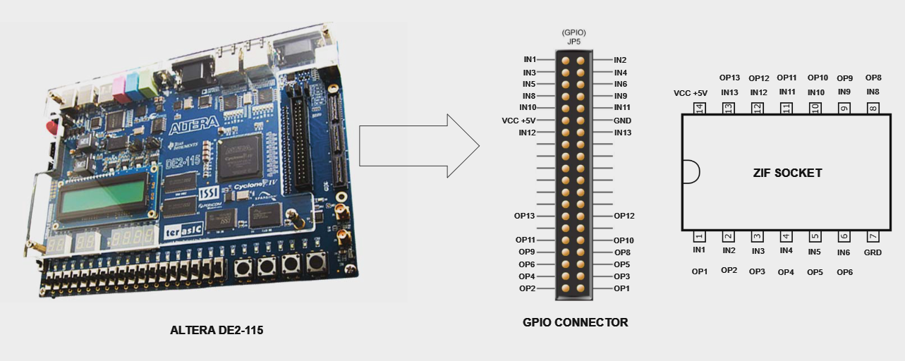
- FPGA Board - Altera DE2-115
- IR Remote
- Jumper Wires
- ZIF Socket
- DUT (Some ICs)
Technology Stack
- FPGA Development Board: ALtera DE2-115
- HDL: Verilog (Hardware Description Language)
- FPGA Synthesis Tool: Quartus II
- Simulation Tool: MultiSim
- Version Control: Git
Bill of Materials (BOM)
| Component Name | Quantity | Unit Cost(LKR) | Cost(LKR) |
|---|---|---|---|
| FPGA Board EP1C3T144 | 1 | 16000 | 16000 |
| Jumper Wires | 30 | 8 | 240 |
| ZIF Socket | 1 | 120 | 120 |
| Testing ICs | 5 | 100 | 500 |
| Total Cost | 16860 |
Solution Architecture
- There is a Zero Insertion Force (ZIF) Socket to configure the IC.
- The FPGA takes the IC number as the User Input through its IR Sensor Module.
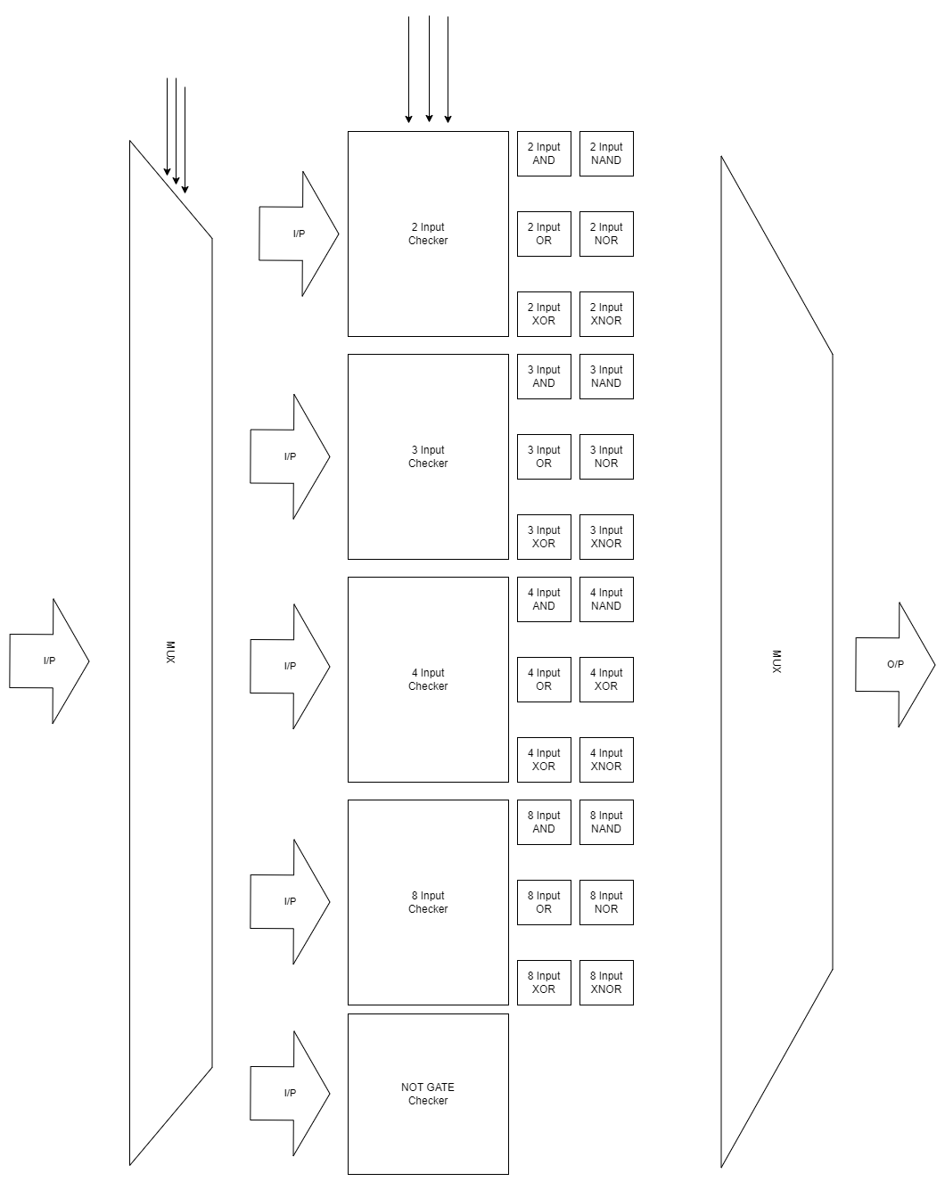
- Then, fetch the related data belonging to that particular IC. That data includes testing patterns, pin configurations, and all required other data.
- Then the FPGA tests the IC with the testing pattern and compares the expected output.
- Finally, display the result and if there is an error indicate the gate that has an error in the LCD board and the Seven Segment display of the FPGA.
Schematics and Diagrams
The main model consists of a KEYPAD, TESTING modules, LCD, SEVEN SEGMENT, and a DUT. Those modules are connected with each other in the following format. The DELAY TESTING module is an extra module and it will be implemented in a later step.
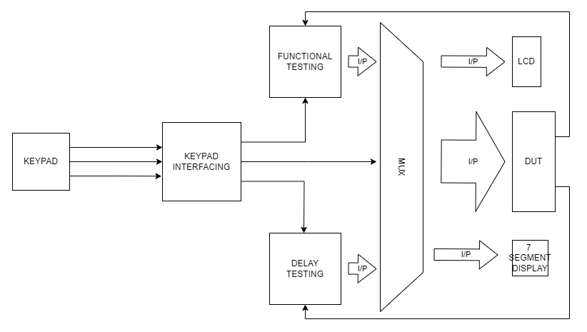
The design of this tester supports 14-pin DIP basic digital logic ICs from the 74 series TTL and CMOS family. The testing model used will be based on the functional fault.
Assembly Instructions
The assembly instructions are as follows. You need to connect the corresponding pins of the GPIO connector to the ZIF Socket as shown in the following figure. Then you can start the FPGA board.
Setup and Configuration
After assigning the PINs correctly, go to the Quartus Project folder on our GitHub page and open the ic_tester QPF file which is located in the ic_tester folder directory. You may use Quartus II 13.1 (64-bit) Web Edition version or another compatible version of Quartus software to open the project file.
All the required things are completed in the project file. If you are using the Altera DE2-115 board, you just need to program the FPGA via Active Serial programming. If you are using another board, the required modification needs to be done accordingly.
Usage
For testing purposes, you just need to enter an IC into the zip socket correctly and enter the IC number using an IR remote. Then the program automatically checks the IC for its logical functionalities and shows the output in the LCD display which is on the Altera DE2-115 board.
Note: For now, this model only works for 74 series logical ICs only. The set of ICs that you can check using this applicaation are listed below.
| IC Number | Function |
|---|---|
| 7400 | Quad 2-input NAND |
| 7402 | Quad 2-input NOR |
| 7403 | Quad 2-input NAND |
| 7408 | Quad 2-input AND |
| 7409 | Quad 2-input AND |
| 7432 | Quad 2-input OR |
| 7438 | Quad 2-input NOR |
| 7486 | Quad 2-input EX-OR |
| 7410 | Triple 3-input NAND |
| 7411 | Triple 3-input AND |
| 7412 | Triple 3-input NAND with open collector outputs |
| 7427 | Triple 3-input NOR |
| 7420 | Dual 4-input NAND |
| 7421 | Dual 4-input AND |
| 7430 | 8-input NAND |
| 7404 | 7404 hex NOT |
| 7405 | Hex NOT with open collector outputs |
| 7414 | Hex NOT with Schmitt trigger inputs |
Safety Considerations
- When you plug the IC, plug it in the correct way. Otherwise, it will damage the IC.
- Before uploading the Quaru project to the board, turn on the programming mode.
…..