Click the thumbnail above to watch the video lecture on YouTube
2.1 Introduction
The evolution of computer technology over the past 50 years has been nothing short of revolutionary. From room-sized scientific calculators to powerful smartphones in our pockets, this transformation has been guided by a prediction made by Intel co-founder Gordon Moore. This lecture examines the technological trends that enabled this revolution, the physical limitations that eventually constrained traditional scaling approaches, and the architectural innovations that emerged in response.
We will trace the exponential growth in transistor density, explore how smaller feature sizes enabled both more complex circuits and faster operation, understand why clock frequencies stopped increasing around 2004, and see how the industry pivoted to multi-core architectures. Finally, we'll examine how computer systems are organized into three layers (hardware, system software, and application software) and follow the complete translation process from high-level code to binary execution.
2.2 Moore's Law - Foundation of Computer Technology Evolution
2.2.1 Who Was Gordon Moore?
Background and Influence:
- Co-founder of Intel Corporation, historically the biggest manufacturer of computer chips/processors
- Most personal computers and high-end servers use Intel processors
- Made a prediction that shaped the entire semiconductor industry
Intel's Dominance:
- Established industry standards for processor design
- Set pace for computational advancement
- Influenced competing manufacturers
- Created benchmark for technology expectations
2.2.2 Moore's Law Definition
The Prediction:
Moore's Law is NOT a physical law like the law of gravity. It is an observation and prediction about technology trends:
"The number of transistors that can be placed on a standard computer chip will double every two years."
Practical Interpretation:
- Roughly translates to: Computational power doubles every two years
- Started in the 1950s and held true for many decades
- Based on continuous demand for increasing computational power
- Self-fulfilling prophecy driven by industry investment
Historical Context:
- Initial observation made in mid-1960s
- Revised and refined over subsequent decades
- Became guiding principle for semiconductor industry
- Influenced research priorities and manufacturing investments
2.2.3 Impact of Moore's Law
Computer Evolution Enabled:
Computers transformed from room-sized scientific calculators to:
- Personal Computers: Desktop and laptop systems in every home
- Mobile Devices: Smartphones with computational power exceeding 1990s supercomputers
- Embedded Systems: Computational intelligence in everyday objects
- Wearables: Smartwatches and fitness trackers
Revolutionary Applications:
Moore's Law made computationally intensive applications possible:
- Human Genome Decoding:
- Massive computational requirements
- Processing billions of genetic sequences
- Pattern recognition across enormous datasets
- World Wide Web and Internet Search:
- Millisecond response times for complex queries
- Indexing billions of web pages
- Real-time information retrieval
- Artificial Intelligence and Machine Learning:
- Neural networks with billions of parameters
- Real-time image and speech recognition
- Autonomous systems and decision-making
- Complex Simulations and Scientific Computing:
- Weather prediction and climate modeling
- Molecular dynamics simulations
- Astrophysical calculations
Societal Impact:
- Computer software became ubiquitous and unavoidable
- Changed how we work, communicate, and learn
- Enabled digital transformation of industries
- Created new fields and destroyed old ones
2.3 Technology Scaling - Historical Data
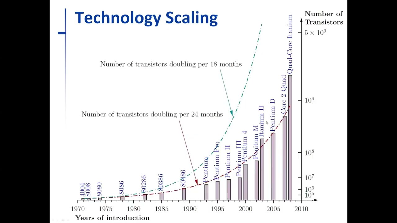
2.3.1 Transistor Count Growth (1970-2010)
Chart Analysis:
The historical data shows remarkable consistency with Moore's prediction:
- Vertical Axis: Number of transistors (10⁵ to 10⁹ - millions to billions)
- Horizontal Axis: Time period (1970 to 2010)
- Blue Dotted Line: Doubling every 18 months (aggressive prediction)
- Red-Brown Line: Doubling every 24 months (Moore's actual prediction)
Real Intel Processor Models:
Tracking actual transistor counts across processor generations:
- Early Processors: 4004, 8008, 8080 (thousands of transistors)
- 1989 Milestone - 8086: Crossed 1 million transistors
- Middle Era: Pentium and Itanium series
- 2008 Achievement: Crossed 1 billion transistors (quad-core processors)
- Trend Validation: Actual counts closely followed the "doubling per 2 years" curve
Significance:
- Prediction held remarkably accurate for 40+ years
- Enabled long-term planning for semiconductor industry
- Guided investment in manufacturing technology
- Set performance expectations for consumers
2.3.2 The x86 Architecture
Origin and Naming:
- 8086 Processor: First x86 architecture processor (notice "86" in the name)
- Established instruction set architecture (ISA) standard
- Created foundation for backward compatibility
x86 Architecture Family:
The architecture evolved through multiple generations while maintaining compatibility:
- 80286: Enhanced memory management
- 80386: True 32-bit processor (author's first computer in 1993, 16 MHz)
- 80486: Integrated floating-point unit
- Pentium Series: Brand name change, performance leap
- Modern Processors: Core i3, i5, i7, i9 series
AMD's Adoption:
- AMD also uses x86 architecture
- Compatible instruction set
- Competitive alternative to Intel
- Drives innovation through competition
Evolution Strategy:
- Architecture evolved significantly over decades
- Maintained backward compatibility throughout
- Old programs run on new processors
- Balanced innovation with stability
2.3.3 Historical Context
Early Computing Era (1985-1990):
- 1985: 80386 computers first arrived on market
- No graphical user interfaces (GUIs) existed
- Black screen with text-only displays
- DOS operating system (text-based console)
- Command-line interaction only
Transformation Period (Mid-Late 1990s):
- GUIs emerged (Windows 95 and similar systems)
- Point-and-click interfaces replaced command lines
- Multimedia capabilities became standard
- Internet connectivity became widespread
User Experience Revolution:
- Significant transformation in how people interacted with computers
- Democratized computing beyond technical experts
- Enabled productivity for non-technical users
- Set expectations for modern computing
2.4 Feature Size Scaling - Lithography Improvements
2.4.1 What Made Transistor Count Increase Possible?
The Answer: Smaller Transistors
The exponential growth in transistor count was enabled primarily by reducing transistor size through improved manufacturing processes.
Lithography Process:
- Etching transistors onto silicon wafer using photolithographic techniques
- Patterns created using light masks and photosensitive materials
- Feature size: Measure of transistor dimensions in nanometers (nm)
- Smaller features = more transistors per unit area
Feature Size Timeline:
The relentless march toward smaller dimensions:
- 2004: 90 nanometer manufacturing process
- 2006: 65 nanometer
- 2008: 45 nanometer (very famous generation, many developments)
- Continuing: 32 nm, 22 nm processes
- 2013 Actual: 22 nm achieved
- 2015 Target: 16 nm achieved
- 2019 Target: 12 nm achieved
- 2023 Target: 7 nm achieved
- 2028 Target: 5 nm exceeded
- Future Roadmap: 3nm and 2nm are currently in production, future is 1nm and sub-1nm
2.4.2 What is "Feature Size"?
Original Definition:
- Originally represented physical measurement: minimum distance between source and drain of transistor
- Also called channel width, gate size, or half-pitch
- Directly related to transistor dimensions
Modern Reality:
- NOT a precisely defined physical measurement anymore
- More of a marketing term in current usage
- General measure of manufacturing process advancement
- Smaller number suggests more advanced technology
Alternative Names:
Different terms referring to approximately the same concept:
- Gate size
- Channel width
- Half-pitch
- Process node
- Technology node
Why Ambiguity Developed:
- Manufacturing processes became more complex
- Multiple dimensions define transistor performance
- 3D structures don't have simple linear measurements
- Marketing convenience over physical precision
2.4.3 How Tiny Are Transistors?
Mind-Boggling Scale:
Putting modern transistor sizes in perspective:
- 45 nanometer technology: Can fit 30 million transistors on the head of a pin
- Across human hair: Over 1,000 transistors fit across the width of a single human hair
- Comparison to past: Incredibly small compared to transistors 40-50 years ago
Manufacturing Precision:
- Requires cleanroom environments cleaner than surgical suites
- Dust particle can destroy multiple chips
- Atomic-level precision required
- Remarkable engineering achievement
2.4.4 Transistor Structure
Basic Components:
- Silicon Substrate: Base semiconductor material
- Source and Drain: Two metal contacts on either side
- Gate: Control electrode positioned between source and drain
- Insulator: Separates gate from channel
Feature Size Definition:
- Distance between drain and source (channel width)
- Critical dimension for transistor operation
- Determines electrical characteristics
Electrical Properties:
- Capacitance Load: Inherent property based on semiconductor material and structure
- Affects switching speed and power consumption
- Function of transistor geometry and materials
- Critical parameter for circuit performance
2.5 Technology Roadmaps - ITRS Predictions
2.5.1 ITRS Organization
International Technology Roadmap for Semiconductors:
- Established: Around 2001
- Purpose: Predict feature size scaling for next 10 years
- Membership: Major semiconductor manufacturers and research institutions
- Methodology: Based on technology capabilities and market demand
Prediction Basis:
The roadmaps considered multiple factors:
- Demand for computational power
- Available manufacturing technology
- Potential technological improvements
- Economic feasibility
- Physical limitations
Regular Updates:
- Produced updated roadmaps regularly
- Adjusted predictions based on actual progress
- Guided industry research priorities
- Dissolved in 2015 due to paradigm shift
2.5.2 Original Roadmap (2001)
Optimistic Projections:
The initial roadmap predicted steady exponential decrease in feature size:
- 2001 Baseline: 130 nm technology in production
- 2006 Target: 65 nm
- 2008 Target: 45 nm
- 2012 Projection: Continuing decrease following Moore's Law
Assumptions:
- Linear continuation of historical trends
- Traditional planar transistor scaling
- Continued improvements in lithography
- Economic sustainability of smaller features
2.5.3 Revised Roadmap (2013)
Adjusted Expectations:
By 2013, reality required revised predictions:
- 2013 Actual: 22 nm achieved
- 2015 Target: 16 nm predicted
- 2019 Target: 12 nm
- 2023 Target: 7 nm
- 2028 Target: 5 nm
Key Observations:
- Rate of reduction slowed down compared to original predictions
- Still following exponential trend but slower pace
- Physical and economic challenges becoming apparent
- Need for alternative approaches emerging
2.5.4 Final Roadmap (2015)
Dramatic Shift in Direction:
The 2015 roadmap marked a fundamental change:
- 2015 Status: Still around 25-24 nm (behind 2013 predictions)
- Near-term Projection: Fast improvements predicted to reach 10 nm
- 2021 Target: 10 nm technology
- Long-term Direction: Feature size would NOT decrease further beyond 10 nm
- Plateau: Would stick with 10 nm for foreseeable future
Significance:
- Sudden departure from decades of continuous scaling
- Recognition of fundamental physical limits
- Industry acknowledgment of new paradigm
- End of traditional Moore's Law scaling
2.5.5 Why the Change? - 3D Technology
Major Paradigm Shift (2013-2015):
The industry pivoted to a fundamentally different approach:
Traditional Approach (Before):
- Single layer of transistors on silicon surface
- Scaling by making transistors smaller
- Two-dimensional planar structures
New Approach (After):
- 3D Chips: Multiple layers of transistors stacked vertically
- 3D FinFET Technology: Transistor fins extending upward from surface
- Vertical Integration: Third dimension for density increase
Impact on Moore's Law:
- Transistor count still increasing (Moore's Law continues)
- But NOT by making individual transistors smaller
- Instead: Stacking transistors on top of each other
- Adds thickness dimension to chip design
Technical Innovations:
- Gate-all-around (GAA) transistors
- Through-silicon vias (TSVs) for vertical connections
- Advanced packaging techniques
- Thermal management solutions
2.5.6 Dissolution of ITRS (2015)
Reasons for Dissolution:
- Technology Divergence: Multiple paths to increase transistor density
- End of Simple Scaling: No longer just reducing feature size
- 3D Stacking: Fundamentally different approach
- Heterogeneous Integration: Combining different technologies on same chip
Multiple Methods for Transistor Density:
Modern approaches include:
- 3D stacking of transistor layers
- FinFET and GAA transistor structures
- Chiplet architectures
- Advanced packaging technologies
- Heterogeneous integration
Moore's Law Status:
- Transistor count still doubling every 2 years (as of 2021)
- But through different means than traditional scaling
- More complex and diverse strategies
- Higher costs per transistor (economic Moore's Law ending)
2.6 Why Smaller Transistors Improve Performance
2.6.1 Reason 1: More Complex Circuits
Increased Transistor Budget:
More transistors available on chip enables more sophisticated functionality.
Comparison Example:
Limited Transistor Count (100 transistors):
- Can only build simple functional units
- Complex tasks must be broken down into simple operations
- Must use simple functional units repeatedly
- Sequential processing of sub-tasks
- Result: SLOWER overall execution
Abundant Transistors (1 billion):
- Can build extremely complex circuits
- Perform complex operations in single step
- Don't need to decompose into simple operations
- Dedicated hardware for sophisticated functions
- Result: FASTER overall execution
Architectural Implications:
- Larger caches for better hit rates
- More sophisticated branch predictors
- Wider execution units (SIMD)
- More parallel functional units
- Hardware accelerators for specific tasks
2.6.2 Reason 2: Faster Switching
Electrical Advantages of Smaller Size:
Smaller transistors possess superior electrical characteristics:
Lower Operating Voltage:
- Smaller channel width requires less voltage to switch transistor
- Voltage scaling: From ~5V (1980s) to ~1V (modern)
- Reduces power consumption
- Enables higher switching frequencies
Reduced Impedance:
- Lower resistance in transistor channel
- Faster current flow
- Quicker charging/discharging of capacitances
Faster State Changes:
- Can switch transistor on/off faster
- Less time needed for signal propagation
- Shorter gate delays
Overall Impact:
- Faster transistor switching → Higher possible clock rate
- Higher clock rate → More operations per second
- Faster overall computation
Physical Explanation:
The relationship between size and speed involves:
- Reduced gate capacitance (smaller area)
- Shorter carrier transit time (shorter channel)
- Lower RC time constants
- Improved frequency response
2.7 Clock Rate Trends - The Power Wall
2.7.1 Clock Rate Increases (1982-2004)
Exponential Growth Era:
Processor clock frequencies increased dramatically for over two decades:
Historical Progression:
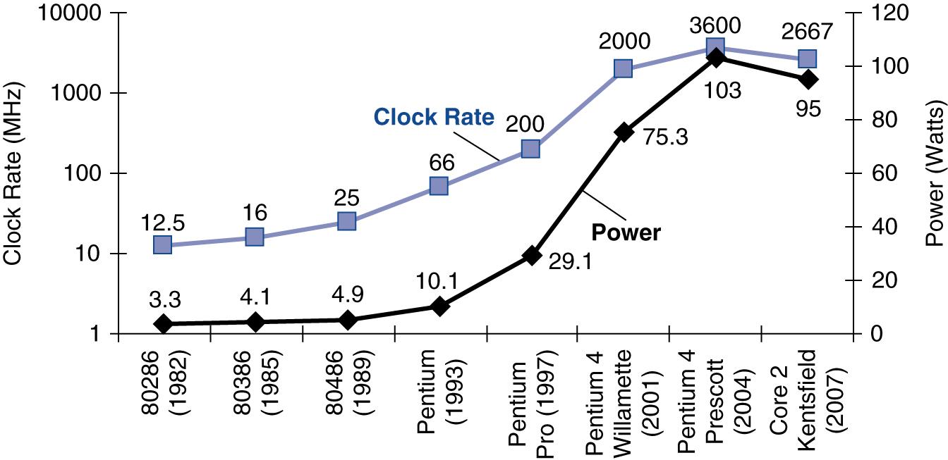
- 286 (1982): 12.5 MHz
- 386 (1985): 16 MHz (author's first computer)
- 486 (Early 1990s): 25-33 MHz
- Pentium (Mid-1990s): 60-200 MHz
- Pentium 4 (2001): 2 GHz (2000 MHz) - First to break 2 GHz barrier
- Pentium 4 Prescott (2004): 3.6 GHz (3600 MHz) - Peak of single-core era
Growth Rate:
- Nearly 300× increase in 20 years
- Roughly doubled every 18-24 months
- Parallel to Moore's Law for transistor count
- Consumer expectation of continuous frequency increases
2.7.2 The Turning Point (2004-2007)
Sudden Deceleration:
Around 2004, the decades-long trend dramatically changed:
- Clock rate increase slowed dramatically
- Reached peak around 3.6-4 GHz
- Settled and plateaued at that level
- Despite transistors continuing to get smaller
The Paradox:
- Manufacturing processes still improving
- More transistors available
- Smaller, potentially faster transistors
- But clock frequencies stopped increasing
Industry Recognition:
- Fundamental limitation encountered
- Alternative approaches needed
- Architectural innovation required
- End of "free" performance scaling
2.7.3 The Power Wall Problem
Power Consumption Growth Crisis:As clock rates increased, power consumption grew unsustainably:
Pentium 4 Prescott Example:
- Required more than 100 watts of power
- Power supply could provide the necessary electrical power
- But HEAT became the critical limiting issue
The Thermal Crisis:
Physical reality of heat generation:
1. Heat Generation Mechanism:- Billions of transistors switching billions of times per second
- Each switching event involves current flow
- Current through resistance generates heat (I²R losses)
- Accumulated heat from all transistors
2. Heat Dissipation Challenge:
- Heat generation outpaced heat removal capability
- Chips would overheat and potentially burn
- Thermal damage to silicon
- Reliability concerns and failure modes
The 100-Watt Rule of Thumb:
Industry consensus emerged:
- Maximum practical limit: ~100 watts per chip
- Cooling solutions couldn't effectively handle more
- Would not cross that boundary for desktop processors
- Required alternative approaches to improve performance
Attempted Solutions (All Insufficient):
Various cooling methods were tried:
- Improved Air Cooling:
- Larger heatsinks
- More powerful fans
- Better thermal interface materials
- Liquid Cooling:
- Water cooling systems (like car radiators)
- More efficient heat transfer
- Complex and expensive
- Exotic Solutions:
- Phase-change cooling
- Thermoelectric coolers
- Ultimately impractical for consumer systems
None Sufficient:
- Couldn't overcome fundamental heat generation problem
- Cost and complexity prohibitive
- Reliability concerns
- Not scalable to mass market
2.7.4 Dynamic Power Equation
The Physics of Power Consumption:Dynamic power consumption follows this relationship:
Factor Analysis (1982-2004):
Capacitance Load:
- Relatively Constant per transistor
- Inherent to transistor structure and materials
- Determined by semiconductor physics
- Cannot be arbitrarily reduced
Voltage Reduction:
- Decreased from ~5V to ~1V
- 5× voltage reduction
- Squared effect: 25× power reduction contribution
- Significant mitigation strategy
Frequency Increase:
- Increased ~300× (12 MHz to 3600 MHz)
- Direct linear effect on power
- 300× power increase contribution
- Overwhelmed voltage reduction benefits
Net Effect Calculation:
Key Insight:
- Despite aggressive voltage scaling (25× reduction in V² term)
- Frequency increase (300×) overwhelmed the benefit
- Net result: Massive power increase
- Power grew faster than could be managed thermally
- Fundamental limitation reached
Why Voltage Couldn't Scale Further:
- Transistor threshold voltages have physical limits
- Signal-to-noise ratio requirements
- Reliability constraints
- Leakage current increases at lower voltages
2.7.5 Overclocking Phenomenon
Marketing and User Community Response:Emerged prominently around early 2000s during the MHz wars:
Manufacturer Approach:
- "Official" Specifications: Conservative clock speed (e.g., 3.6 GHz)
- Actual Capability: Could run at higher speeds without guarantees
- Marketing Tactic: Appeal to gamers and power users
- Risk Disclaimer: No warranty at higher speeds
User Overclocking:
Users could manually increase clock speed beyond rated specification:
Process:
- Change BIOS/UEFI settings
- Increase multiplier or bus speed
- Often increase voltage
- Improve cooling solutions
Risks:
- Generate More Heat: Exceed thermal design power (TDP)
- Potential Damage: Could permanently destroy processor
- Instability: System crashes and data corruption
- Reduced Lifespan: Accelerated aging of components
- Voided Warranty: No manufacturer support
Target Audience:
- Gamers: Seeking maximum frame rates
- Enthusiasts: Hobbyists and competitors
- Overclockers: Specialized community
- Benchmarkers: Competitive performance testing
Industry Impact:
- Created enthusiast market segment
- Influenced product differentiation (K-series Intel chips)
- Added revenue from premium products
- Many processors destroyed but market remained
2.8 Shift to Multi-Core Processors
2.8.1 The Challenge
The Industry Dilemma:
By mid-2000s, the semiconductor industry faced a paradox:
Available Resources:
- Moore's Law still valid: More transistors available every generation
- Manufacturing processes continuing to improve
- Silicon area increasing or transistor density growing
Constraints:
- Cannot use all transistors simultaneously (power wall/heat problem)
- Cannot increase clock rate (thermal limitations)
- Traditional performance scaling broken
Critical Questions:
- How to utilize available transistors?
- How to continue improving computational power?
- How to maintain Moore's Law performance benefits?
2.8.2 Solution: Multiple Processor Cores
Paradigm Shift (2004-2008):Industry pivoted from single-core to multi-core architectures:
Core Concept:
Instead of one powerful processor, put multiple complete processors on same chip:
- Each core is a complete CPU
- Cores share cache and memory interface
- Can execute different programs simultaneously
- Parallel execution at thread/process level
Early Multi-Core Processors:
AMD Barcelona (2007):
- 4 cores on single die
- Shared L3 cache
- Integrated memory controller
Intel Core Series:
- Multiple models with 4 cores
- Hyperthreading technology (2 threads per core)
- Competitive performance
IBM Processors:
- Server-oriented multi-core designs
- High core counts for enterprise
- Power-efficient designs
Extreme Designs:
- Some manufacturers: 8 cores per chip
- Specialized server processors with more
- Graphics processors (GPUs) with hundreds of simple cores
Power Management:
- Dynamic Power Allocation: Cores powered on/off as needed
- Turbo Boost: Temporarily increase frequency of active cores
- Per-Core Voltage/Frequency Scaling: Independent control
- Power Gating: Completely shut down unused cores
- Thermal Management: Distribute heat across die
2.8.3 The Plan
Initial Industry Vision:
Following Moore's Law principle for core counts:
Projected Growth:
- Every 2 years: Double the number of cores per chip
- Use increased transistor budget for more cores
- Each generation: 2× cores, same power envelope
Timeline Projection:
- 2006: 4 cores
- 2008: 8 cores
- 2010: 16 cores
- 2012: 32 cores
- 2014: 64 cores
- By 2021: Should have hundreds of cores in consumer processors
Theoretical Benefits:
- Continuous performance improvement
- Utilizing Moore's Law transistor growth
- Working within power constraints
- Parallel computing becoming mainstream
Reality Check:
- This did NOT happen
- Current consumer chips: Typically 4-16 cores (2021)
- Server processors: Up to 64-128 cores
- Not the hundreds predicted
- Growth much slower than initial projections
2.8.4 Why Multi-Core Growth Slowed
The Fundamental Problem: Parallel Programming Difficulty
Software Challenge:
Multi-core processors require fundamentally different programming approach:
Sequential Programming (Traditional):
- Single thread of execution
- One operation after another
- Natural mental model
- Straightforward debugging
- Predictable behavior
Parallel Programming (Required for Multi-Core):
- Multiple simultaneous threads of execution
- Programmer must explicitly write code for multiple processors
- Must think: "I'm writing for 4, 8, or 16 processors"
- Coordinate and synchronize multiple processes/threads
- Manage shared resources and data
Available Parallel Programming Techniques:
Multi-Threading:
- POSIX Threads (pthreads) in C/C++
- Java threading primitives
- Python threading/multiprocessing
- Operating system thread scheduling
Multiple Processes:
- Fork/join models
- Message passing (MPI for scientific computing)
- Process pools
Communication Mechanisms:
- Shared memory
- Message queues
- Pipes and sockets
- Synchronization primitives (mutexes, semaphores, barriers)
Language Support:
- Available in most major programming languages
- Library support varies in quality
- Language-level primitives vs library-based approaches
Inherent Difficulties:
1. Parallel Programming is HARD:
- Much more difficult than sequential programming
- Different mental model required
- Non-deterministic behavior
- Difficult to reproduce bugs
- Race conditions and deadlocks
2. Requires Deep Understanding:
- Hardware Architecture: How cores communicate, cache coherency
- Processor Organization: Memory hierarchy, interconnects
- Communication Overhead: Cost of data transfer between cores
- Synchronization Overhead: Cost of coordinating execution
Key Technical Challenges:
Load Balancing:
- Problem: Distribute work evenly across all cores
- Bad Scenario: One processor idle while another overloaded
- Requirement: Dynamic or static work distribution
- Complexity: Workload often unknown until runtime
- Solution Difficulty: NP-hard problem in general case
Communication Optimization:
- Problem: Minimize data transfer between cores
- Reality: Communication takes time (overhead)
- Amdahl's Law: Communication is sequential bottleneck
- Cache Coherency: Hardware protocol overhead
- Solution: Locality-aware algorithms, minimize sharing
Synchronization:
- Problem: Coordinate execution between cores
- Bad Scenario: One thread waiting indefinitely for another
- Overhead: Synchronization primitives have cost
- Deadlock Risk: Circular dependencies can halt system
- Solution: Careful design, lock-free algorithms
Performance Consequences:
If parallel programming not done well:
- Wasting Available Hardware: Cores sitting idle
- No Performance Gain: Sequential sections dominate
- Worse Performance: Overhead exceeds benefits
- Unpredictable Results: Race conditions cause incorrect output
2.8.5 Instruction-Level Parallelism vs Multi-Core Parallelism
Instruction-Level Parallelism (ILP):
Characteristics:
- Hardware-Based Solution: Processor automatically finds parallelism
- Automatic Execution: Fetches multiple instructions simultaneously
- Out-of-Order Execution: Reorders for efficiency
- Compiler Support: Helps but not required
- Transparent to Programmer: No special code needed
- Automatic and Hidden: Works without programmer awareness
Techniques:
- Superscalar execution
- Out-of-order execution
- Register renaming
- Speculative execution
- Branch prediction
Benefits:
- Free performance improvement
- Works on existing sequential code
- No programmer burden
- Automatic optimization
Multi-Core Parallelism:
Characteristics:
- Explicit Programming Required: Programmer must manually parallelize
- Not Automatic: No hardware magic
- Much More Difficult: Requires expertise
- Programmer Responsibility: Must handle all coordination
Programmer Must:
- Break program into parallel threads
- Distribute work across cores
- Handle inter-core communication
- Manage synchronization
- Deal with race conditions
- Avoid deadlocks
- Balance load
- Minimize communication overhead
Contrast:
| Aspect | ILP | Multi-Core |
|---|---|---|
| Who does work | Hardware | Programmer |
| Transparency | Invisible | Explicit |
| Difficulty | Automatic | Hard |
| Applicability | All code | Limited patterns |
| Overhead | Hidden | Must manage |
2.8.6 Impact on Software Development
For Regular Programmers:
- Too Difficult: Most cannot effectively parallelize
- Not Worth Effort: For many applications
- Sequential Sufficient: Many programs don't need parallel performance
- Training Gap: Most programmers not trained in parallel programming
For Computer Engineers:
- Essential Skill: Must learn parallel programming
- Career Requirement: High-performance computing demands it
- Necessary Understanding: Must understand hardware deeply
- Specialized Constructs: Must master threading, synchronization
- Architecture Knowledge: Must understand cache coherency, memory models
Application Domains:
High-Performance Applications Requiring Parallelism:
- Scientific computing and simulations
- Video encoding/decoding
- Machine learning training
- Real-time graphics rendering
- Big data processing
- Financial modeling
Applications That Remain Sequential:
- Many business applications
- Simple utilities
- I/O-bound programs
- Interactive applications
- Legacy software
Education Impact:
- Computer science curricula adding parallel programming courses
- Need for hardware architecture understanding
- Gap between industry needs and graduate preparation
- Specialized training for HPC (high-performance computing)
2.9 Computer System Organization - Three Layers
2.9.1 Hardware Layer (Bottom)
Physical Components:
Processor (CPU):
- Central Processing Unit
- Executes machine instructions
- Contains control and datapath
- Includes registers and functional units
Microarchitecture:
- Internal organization of processor
- Pipeline structure
- Execution units
- Cache organization
- Bus interfaces
Memory Hierarchy:
- Level 1 Cache (L1):
- Smallest, fastest
- Separate instruction and data caches
- On-core, immediate access
- Typically 32-64 KB per core
- Level 2 Cache (L2):
- Larger, slightly slower
- May be shared or per-core
- Typically 256 KB - 1 MB per core
- Level 3 Cache (L3):
- Largest, slower than L2
- Shared across all cores
- Typically several MB
- Main Memory (RAM):
- Dynamic RAM (DRAM)
- Several GB capacity
- Much slower than cache
- Volatile storage
Input/Output Controllers:
- USB controllers
- Network interfaces
- Display adapters
- Storage controllers
Secondary Storage Interfaces:
- SATA for hard drives/SSDs
- NVMe for fast SSDs
- External storage connections
Purpose:
- Actual physical components that execute computation
- Store and retrieve data
- Interact with peripherals and external world
- Provide computational substrate
2.9.2 System Software Layer (Middle)
Tool Chain Components:Compiler:
- Function: Translates high-level language to assembly
- Input: Source code (C, Java, Python, etc.)
- Output: Assembly language or intermediate representation
- Optimization: Improves performance, reduces size
- Examples: GCC, Clang, MSVC, Javac
Assembler:
- Function: Translates assembly to machine code
- Input: Assembly language (human-readable mnemonics)
- Output: Object files (binary machine code)
- Tasks: Symbol resolution, address assignment
- Examples: GNU Assembler (as), NASM
Linker:
- Function: Combines object files and libraries
- Tasks: Resolves external references, creates executable
- Output: Complete executable program
- Link Types: Static linking, dynamic linking
- Examples: GNU ld, MSVC linker
Purpose of Tool Chain:
- Support application development
- Bridge high-level abstractions to machine code
- Enable programmer productivity
- Provide optimization opportunities
Operating System:
Core Responsibilities:
Resource Management:
- CPU time allocation
- Memory space allocation
- I/O device arbitration
- Storage space management
Memory Management:
- Virtual memory implementation
- Page tables and address translation
- Memory protection between processes
- Swap space management
Storage Management:
- File system implementation
- Directory structures
- File permissions and security
- Disk block allocation
Input/Output Handling:
- Device drivers
- Interrupt handling
- Buffering and caching
- Asynchronous I/O
Task Scheduling:
- Process scheduling algorithms
- Thread scheduling
- Priority management
- Time-slicing and preemption
Resource Sharing:
- Prevents conflicts between programs
- Enforces isolation
- Provides controlled sharing mechanisms
Why Operating System Needed:
Trust and Security:
- Cannot trust application software
- Programs can be malicious or buggy
- Programs don't consider other programs
- Need supervision and enforcement
Coordination and Protection:
- Prevents programs from breaking hardware
- Enforces rules set by hardware (privileged instructions)
- Provides abstraction hiding hardware details
- Mediates access to shared resources
Programmer Benefits:
Abstractions Provided:
Programmers don't need to worry about:
- Where program code resides in physical memory
- Where variables are stored in RAM
- Hardware resource conflicts
- Direct hardware access
- Physical device characteristics
OS Guarantees:
- Safe hardware usage
- Process isolation
- Consistent interfaces
- Reliable file storage
- Network communication
Example Services:
- File I/O without knowing disk geometry
- Memory allocation without physical addresses
- Network communication without protocol details
- Device I/O without hardware specifics
2.9.3 Application Software Layer (Top)
User-Level Programs:
- Programs written by application programmers
- Solve specific problems or provide services
- Interact with users
- Implement business logic
High-Level Programming Languages:
Popular Languages:
- C: Systems programming, performance-critical
- Java: Enterprise applications, portability
- Python: Scripting, data science, machine learning
- R: Statistical analysis, data science
- JavaScript: Web development, client-side
- C++: Performance with abstraction
- Go: Concurrent systems, cloud services
- Rust: Systems programming, memory safety
Language Characteristics:
Hundreds/Thousands Available:
- Each optimized for specific application domains
- Different paradigms (imperative, functional, object-oriented)
- Trade-offs between performance and productivity
- Community and ecosystem considerations
Domain Optimization:
- Machine Learning: Python (NumPy, TensorFlow, PyTorch), R
- Systems Programming: C, C++, Rust
- Enterprise Applications: Java, C#
- Web Development: JavaScript, TypeScript, PHP, Ruby
- Scientific Computing: Python, Julia, MATLAB, Fortran
- Mobile Development: Swift, Kotlin, Java
- Game Development: C++, C#
Level of Abstraction:
- Represents algorithms and solutions to problems
- Closest to problem domain
- Furthest from hardware details
- Highest productivity for programmers
- Requires compilation/interpretation to execute
2.10 From High-Level Code to Machine Code - The Translation Process
2.10.1 Example: Swap Function in C
Source Code:
void swap(int v[], int k) {
    int temp;
    temp = v[k];
    v[k] = v[k+1];
    v[k+1] = temp;
}
Function Purpose:
- Operation: Swap two values in array
- Parameters:
v[]: Array pointer (base address)k: Index of first element to swap
- Elements Swapped: Positions k and k+1
- Method: Uses temporary variable
- Simplicity: Basic operation used frequently in sorting algorithms
Algorithm:
- Store
v[k]in temporary variable - Copy
v[k+1]tov[k] - Copy temporary to
v[k+1]
2.10.2 After Compilation - MIPS Assembly Code
Assembly Translation:
The compiler generates 7 MIPS instructions to implement the swap function:
MUL  $2, $5, 4      # Multiply k by 4 (array index to byte offset)
ADD  $2, $4, $2     # Add base address to offset (address of v[k])
LW   $15, 0($2)     # Load v[k] into register $15 (temp = v[k])
LW   $16, 4($2)     # Load v[k+1] into register $16
SW   $16, 0($2)     # Store v[k+1] to v[k]
SW   $15, 4($2)     # Store temp to v[k+1]
Translation Analysis:
- 5 C statements → 7 assembly instructions
- Expansion due to instruction granularity
- Each assembly instruction is simple operation
Key Operations Explained:
1. Address Calculation:
- Multiply by 4: Each integer occupies 4 bytes in memory
- Index k must be converted to byte offset (k×4)
- Calculate memory address of v[k]
2. Memory Addressing:
- Base address of array in register $4
- Offset calculated and added to base
- Results in absolute memory address
3. Register Usage:
- $4: Base address of array v (parameter)
- $5: Value of k (parameter)
- $2: Temporary register for address calculation
- $15: Temporary storage for v[k] value
- $16: Temporary storage for v[k+1] value
Instruction Set Details:
- MIPS ISA used in example (not ARM, but similar concepts)
- Load-Store architecture
- Register-to-register operations
- Explicit memory addressing
2.10.3 After Assembly - Machine Code
Binary Representation:
Each assembly instruction translates to 32-bit binary instruction:
00000000101000100001000000011000  # MUL $2, $5, 4
00000000100000100001000000100001  # ADD $2, $4, $2
10001100010011110000000000000000  # LW  $15, 0($2)
10001100010100000000000000000100  # LW  $16, 4($2)
10101100010100000000000000000000  # SW  $16, 0($2)
10101100010011110000000000000100  # SW  $15, 4($2)
One-to-One Mapping:
- Each assembly instruction → Exactly one 32-bit machine instruction
- No information lost or gained
- Deterministic translation
- Assembly is human-readable form of machine code
Instruction Format:
Different instruction types have different bit field layouts:
R-Type (Register) Format:
[Opcode 6 bits][Rs 5 bits][Rt 5 bits][Rd 5 bits][Shamt 5 bits][Funct 6 bits]
I-Type (Immediate) Format:
[Opcode 6 bits][Rs 5 bits][Rt 5 bits][Immediate 16 bits]
Instruction Components Specify:
- Opcode: Operation category
- Destination Register: Where result goes
- Source Registers: Where operands come from
- Immediate Values: Constant values (like 4 in multiply)
- Function Code: Specific operation for R-type
Example Analysis:
In the immediate value 4:
- Appears in specific bit positions
- Encoded in binary (00000000000100)
- Part of instruction encoding
Binary Image:
- Complete program represented as sequence of 32-bit words
- Called executable or binary image
- Stored in secondary storage (hard disk, SSD)
- Loaded into memory when program executes
- CPU fetches and executes instructions sequentially
2.11 Program Execution - Inside the CPU
2.11.1 Block Diagram of Computer
System Components:
Compiler/Tool Chain:
- Translates human-written program to machine code
- Optimization and code generation
- Produces executable binary
Memory:
- Stores program instructions
- Stores program data
- Hierarchical (cache, RAM, disk)
CPU (Central Processing Unit):
- Executes machine instructions
- Performs arithmetic and logic
- Controls program flow
Input/Output:
- Peripherals (keyboard, display, network)
- Storage devices (disk, SSD)
- Communication interfaces
Program Execution Flow:
1. Compile Stage:
- Source code → Assembly → Machine code
- Performed once (or when code changes)
- Output: Executable binary file
2. Store Stage:
- Machine code saved to secondary storage
- Persistent storage (survives power off)
- Typically on hard disk or SSD
3. Load Stage:
- Machine code loaded into main memory (RAM) when program runs
- Operating system performs loading
- Program becomes "process"
4. Execute Stage:
- CPU fetches instructions from memory one by one
- Executes each instruction in sequence (or out-of-order)
- Updates registers and memory
5. Results Stage:
- Computed values stored back in memory
- Output sent to I/O devices
- Results displayed or saved
2.11.2 Inside the CPU - Two Main Components
Datapath:
Structure:
- Collection of logic circuits interconnected
- Forms a path through CPU
- Instruction and data travel through this path
- Sequential stages of processing
Components:
- Functional units (adders, multipliers, shifters, logic units)
- Registers for temporary storage
- Multiplexers for routing
- Buses for data transfer
Function:
- Instruction travels from one logic circuit to another
- Each circuit performs specific operation on data
- Transforms inputs to outputs
- Executes the computational work
Examples of Functional Units:
- Arithmetic Logic Unit (ALU)
- Floating-Point Unit (FPU)
- Load-Store Unit
- Branch Unit
Control:
Structure:
- Another logic circuit (or set of circuits)
- Generates control signals
- Coordinates datapath operation
Function:
- Governs instruction/data flow through datapath
- Ensures instructions execute correctly
- Selects appropriate functional units
- Controls multiplexers and enables
Responsibilities:
- Decode instructions
- Generate appropriate control signals
- Coordinate timing
- Handle exceptions and interrupts
Interaction:
- Control tells Datapath what to do
- Datapath performs the actual computation
- Control monitors Datapath status
- Together implement instruction execution
2.11.3 Execution Process (Conveyor Belt Analogy)
Instruction Execution Cycle:
1. Fetch:
- Instructions stored in memory
- Control fetches one instruction at a time
- Brings instruction into CPU
- Increments program counter
2. Decode:
- Instruction enters datapath
- Control decodes instruction
- Determines operation type
- Identifies operands
3. Execute:
- Instruction travels through logic circuits in datapath
- Operations performed on data
- Functional units activated
- Intermediate results produced
4. Memory:
- Memory accesses performed if needed (load/store)
- Data read from or written to memory
- Address calculation completed
5. Writeback:
- Results generated
- Written back to registers
- Results may be sent to memory or I/O
6. Repeat:
- Cycle repeats for next instruction
- Like conveyor belt: continuous flow
- One instruction after another (in simple model)
Conveyor Belt Metaphor:
- Instructions like items on conveyor belt
- Each station performs specific operation
- Continuous movement through system
- Pipelining overlaps multiple instructions (discussed in later lectures)
2.11.4 Cache Memory
Purpose and Motivation:
The Performance Gap:
- CPU can process data very fast
- Main memory access is relatively slow
- Speed mismatch creates bottleneck
- CPU would waste time waiting for memory
Cache Solution:
- Fast memory located on CPU chip
- Very close to processor core physically
- Stores copies of frequently used instructions and data
- Exploits locality of reference
Cache Hierarchy:
Level 1 Cache (L1):
- Smallest capacity (32-64 KB)
- Fastest access (1-2 cycles)
- Closest to core
- Often split: L1-I (instruction), L1-D (data)
Level 2 Cache (L2):
- Medium capacity (256 KB - 1 MB)
- Medium access time (4-10 cycles)
- May be per-core or shared
- Unified (instructions and data)
Level 3 Cache (L3):
- Largest capacity (several MB)
- Slower access (20-40 cycles)
- Shared across all cores
- Last level cache (LLC)
Performance Impact:
- Cache hit: Data found in cache (fast)
- Cache miss: Must access main memory (slow)
- Hit rate critical for performance
- Well-designed cache can achieve >95% hit rate
Will Learn in Lecture:
- Cache organization
- Mapping strategies (direct-mapped, set-associative)
- Replacement policies
- Write policies
- Cache coherency in multi-core
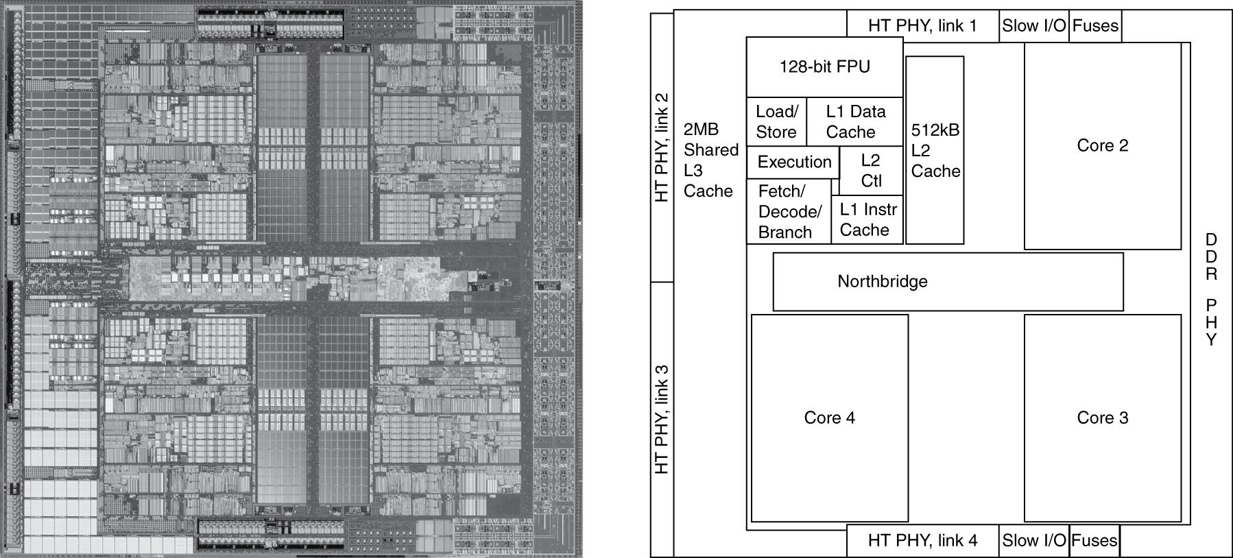
2.12 Real CPU Layout - AMD Barcelona Example
2.12.1 Overview
AMD Barcelona Processor:
- Released around 2007
- Quad-core processor (4 cores on single die)
- 65nm manufacturing process
- Actual chip much smaller than magnified images
- Can visually identify individual components
Die Photo Analysis:
- Optical or electron microscope image
- Shows physical layout of components
- Different functional units visible
- Reveals organizational decisions
- Educational value for understanding architecture
2.12.2 Four Processor Cores
Core Distribution:
Physical layout shows clear quadrant organization:
- Core 1: Upper left area of die
- Core 2: Upper right area of die
- Core 3: Lower left area of die
- Core 4: Lower right area of die
Layout Strategy:
- Mirror Image Layouts: Cores identical but mirrored
- Symmetry: Simplifies design and manufacturing
- Thermal Distribution: Spreads heat across die
- Interconnect Balance: Equal distances to shared resources
2.12.3 Inside Each Core
Floating-Point Unit (FPU):
Characteristics:
- Large Component: Significant silicon area in each core
- Complex Circuitry: Handles IEEE 754 floating-point arithmetic
- High Transistor Count: Precision requires many gates
Operations:
- Addition, subtraction of floating-point numbers
- Multiplication of floating-point numbers
- Division of floating-point numbers
- Square root and other mathematical functions
Why So Large:
- Floating-point math more complex than integer
- Requires normalization, rounding, exception handling
- Multiple pipeline stages
- High precision demands
Load-Store Unit:
Function:
- Handles all memory operations
- Loads data from memory to CPU registers
- Stores data from CPU registers to memory
- Critical for data transfer
Operations:
- Address calculation
- Cache access
- TLB (Translation Lookaside Buffer) lookup
- Memory ordering and consistency
Integer Execution Unit:
Characteristics:
- Smaller than FPU: Integer operations generally simpler
- High Frequency: Often faster than floating-point
Operations:
- Integer arithmetic (add, subtract, multiply, divide)
- Bitwise logical operations (AND, OR, XOR, NOT)
- Shifts and rotates
- Comparisons
Why Smaller:
- Simpler algorithms
- No normalization needed
- Exact arithmetic (no rounding)
- Fewer pipeline stages
Fetch and Decode Unit:
Responsibilities:
Instruction Fetch:
- Fetches instructions from memory (via I-cache)
- Predicts branch targets
- Manages instruction buffer
Instruction Decode:
- Makes sense of binary instruction encoding
- Determines instruction type
- Identifies operands
- Generates micro-ops (for CISC architectures)
Pipeline Frontend:
- Prepares instructions for execution
- Handles instruction-level parallelism
- Feeds execution units
Level 1 Data Cache (L1 D-Cache):
Characteristics:
- Stores frequently used data (not instructions)
- Very fast access (1-2 cycle latency)
- Close to execution units
- Separate from instruction cache (Harvard architecture)
Typical Specifications:
- 32-64 KB capacity
- 8-way set associative
- Write-through or write-back policy
Level 1 Instruction Cache (L1 I-Cache):
Characteristics:
- Stores frequently used instructions (program code only)
- Very fast access
- Feeds fetch unit
- Separate from data cache
Benefits of Separation:
- No structural hazards (simultaneous instruction fetch and data access)
- Optimized for different access patterns
- Simpler control logic
Level 2 Unified Cache (L2 Cache):
Characteristics:
- Larger than L1: Typically 512 KB per core in Barcelona
- Stores both instructions and data (unified)
- Further from execution units (higher latency)
- Victim cache for L1 misses
Architecture:
- Dedicated control logic for coherency
- Interface to L3 cache or memory
- May use different associativity than L1
2.12.4 Shared Components
North Bridge (Central Hub):
Location:
- Central/middle area of chip
- Strategic position for communication
Functions:
- L2-to-Memory Connection: Connects all L2 caches to main memory
- Inter-Core Communication: Coordinates between cores
- Memory Controller: May include integrated memory controller
- Cache Coherency: Maintains coherency protocol between cores
Critical Role:
- Central communication circuit
- Bandwidth bottleneck if not designed well
- Affects multi-core scaling
DDR PHY (Physical Controller):
DDR Memory:
- DDR: Dual Data Rate SDRAM
- Transfers data on both rising and falling clock edges
- Industry-standard memory interface
PHY (Physical Layer):
- PHY: Physical layer controller
- Interfaces CPU to DDR RAM modules
- Handles physical signaling
Responsibilities:
- Electrical interface to memory chips
- Signal timing and termination
- Training and calibration
- Error detection/correction
HyperTransport Controllers:
HyperTransport Technology:
- High-speed interconnect technology (AMD proprietary)
- Point-to-point serial communication
- Replaces legacy parallel buses
- High bandwidth, low latency
Connections:
- External Devices: Graphics cards, other processors
- Chipset Communication: Northbridge, southbridge links
- I/O Device Connectivity: Network, storage, peripherals
Benefits:
- Scalable bandwidth
- Lower pin count than parallel buses
- NUMA (Non-Uniform Memory Access) support for multi-socket systems
2.12.5 Additional Information
WikiChip Database: https://en.wikichip.orgComprehensive Processor Information:
Major Manufacturers Covered:
- Intel Processors: x86 architecture, Core series, Xeon servers
- AMD Processors: x86 architecture, Ryzen, EPYC, Threadripper
- ARM Processors: Mobile devices, embedded systems, servers
- Samsung Exynos: Smartphones and tablets
- Apple A-Series: iPhone and iPad processors
- Apple M-Series: Mac computers (ARM-based)
- Qualcomm: Snapdragon mobile processors
- NVIDIA, Broadcom, Texas Instruments, and many more
Available Information:
Visual Content:
- Processor die photographs and diagrams
- Block diagrams showing architecture
- Cache hierarchy visualizations
- Microarchitecture pipeline diagrams
Technical Specifications:
- Manufacturing process (nm technology)
- Transistor counts and density
- Transistor types and structures
- Die size and area
- Power consumption (TDP)
- Clock speeds (base and turbo)
- Core counts and threading
- Cache sizes and organization
Advanced Topics:
- 3D stacking technology details
- FinFET and GAA transistor structures
- Packaging technologies
- Memory interface specifications
- I/O capabilities
Current Technology Landscape (2021):
Mainstream Manufacturing:
- 10 nm and 7 nm processes in volume production
- Multiple manufacturers at this node
Future Direction:
- Next Few Years: Shift to 5 nm and 3 nm
- 2 nm and 1 nm in research
Important Clarification:
- Numbers don't represent actual gate size anymore
- Marketing terms more than physical measurements
- Example: 5 nm transistors may have wider channels than 10 nm
- Density Increase Through:
- 3D stacking (vertical integration)
- FinFET and GAA structures
- Improved layouts and design rules
- Multi-patterning lithography
Key Takeaways
- Moore's Law predicted transistor doubling every 2 years - remarkably accurate for over 40 years, guiding semiconductor industry planning and investment
- Smaller transistors enabled by improved lithography - progression from 90nm → 45nm → 22nm → 7nm → 5nm through advancing manufacturing processes
- Feature size now marketing term rather than physical measurement - modern processes use 3D structures making simple linear dimensions misleading
- Smaller transistors provide dual benefits - enable more complex circuits (more transistors available) and faster switching (lower voltage, reduced impedance)
- Clock rate increased exponentially until ~2004 - grew from 12.5 MHz (1982) to 3.6 GHz (2004), then hit fundamental thermal limitations
- Power wall halted frequency scaling - heat generation (
P = CV²f) exceeded cooling capability, establishing ~100W practical limit for consumer processors - Dynamic power equation explains the crisis - despite 25× power reduction from voltage scaling, 300× frequency increase overwhelmed the benefit
- Overclocking emerged as risky performance technique - users could exceed rated speeds at risk of destroying processors, popular among gaming enthusiasts
- Industry pivoted to multi-core processors - solution to utilize Moore's Law transistors without exceeding power limits, starting ~2004-2008
- Multi-core growth slowed due to programming difficulty - initial projection of hundreds of cores didn't materialize; parallel programming remains challenging
- Parallel programming requires explicit management - unlike automatic instruction-level parallelism, multi-core requires programmers to handle threads, synchronization, communication
- Three major parallel programming challenges - load balancing across cores, minimizing communication overhead, optimizing synchronization
- 3D chip technology changed scaling paradigm (2013-2015) - industry shifted from pure 2D shrinking to vertical stacking of transistor layers
- ITRS dissolved in 2015 - technology roadmap organization ended as multiple paths to density replaced simple feature size scaling
- Computer systems organized in three layers - hardware (physical components), system software (OS, compilers, tools), application software (user programs)
- System software provides abstraction and protection - OS prevents malicious programs from damaging hardware, hides complexity from application programmers
- Program translation is multi-stage process - high-level language → assembly language → machine code through compiler, assembler, linker
- CPU contains datapath and control - datapath performs computation by routing data through functional units; control coordinates execution and generates signals
- Cache memory critical for performance - fast on-chip memory (L1, L2, L3) stores frequently accessed data/instructions, hiding main memory latency
- Real CPUs have complex layouts - die photos reveal intricate organization with multiple cores, cache hierarchies, shared interconnects, memory controllers
Summary
This lecture provides a comprehensive examination of computer technology evolution from the 1970s to present day. Moore's Law, predicting transistor count doubling every two years, serves as the guiding principle for the semiconductor industry and enables the transformation of computers from room-sized machines to powerful pocket devices.
The progression of manufacturing technology steadily reduced feature sizes from 90 nanometers to current 7nm and 5nm processes. Smaller transistors provided two key advantages: more transistors per chip enabling complex functionality, and faster switching speeds enabling higher clock frequencies. Clock rates grew exponentially from 12.5 MHz in 1982 to 3.6 GHz in 2004.
However, around 2004, the industry encountered the power wall - a fundamental thermal limitation. The dynamic power equation (P = CV²f) revealed that despite aggressive voltage scaling, the massive frequency increases caused power consumption and heat generation to exceed cooling capabilities. The ~100-watt limit for consumer processors could not be overcome by improved cooling solutions.
The solution was multi-core processors: placing multiple complete CPU cores on a single chip. This allowed continued performance improvement within power constraints by exploiting thread-level parallelism. However, the initial vision of exponentially growing core counts didn't materialize due to the difficulty of parallel programming. Unlike automatic instruction-level parallelism, multi-core requires programmers to explicitly manage threads, balance loads, minimize communication, and handle synchronization - a significantly more challenging paradigm.
Around 2013-2015, the industry made another major shift to 3D chip technology. Instead of only shrinking transistors in two dimensions, manufacturers began stacking transistor layers vertically using FinFET and similar technologies. This represented such a fundamental change that the International Technology Roadmap for Semiconductors (ITRS) dissolved in 2015, as simple feature-size predictions no longer captured the diverse approaches to increasing transistor density.
The lecture concluded by examining computer system organization across three layers: hardware (processor, memory, I/O), system software (compilers, assemblers, operating system), and application software (programs written in high-level languages). We traced the complete journey from high-level code through compilation and assembly to binary machine code, and explored how programs execute through the interaction of control and datapath components within the CPU. Cache memory's critical role in hiding main memory latency was emphasized, and real-world processor layouts illustrated the complex organization of modern multi-core chips.
Understanding these technology trends and architectural responses provides essential context for studying computer architecture and explains why processors are organized as they are today.