Click the thumbnail above to watch the video lecture on YouTube
9.1 Introduction
This lecture transitions from instruction set architecture (ISA) to microarchitecture—the hardware implementation of the ISA. We explore how to build a processor that executes MIPS instructions, covering instruction formats, digital logic fundamentals, datapath construction, and single-cycle processor design. Understanding microarchitecture reveals how software instructions translate to hardware operations and provides the foundation for studying advanced processor designs including pipelining and superscalar execution.
9.2 MIPS ISA
9.2.1 Transition to Hardware Implementation
Previous Focus: ARM ISA
- Instruction set
- Assembly programming
- Software perspective
Current Focus: MIPS Microarchitecture
- Hardware implementation
- Processor design
- Hardware perspective
Why MIPS for Hardware Study?
- Simpler than ARM (educational clarity)
- Clean RISC design
- Well-documented architecture
- Concepts apply to all processors
9.2.2 MIPS Instruction Categories
Three Instruction Types (based on encoding)
I-Type (Immediate)
- Contains one immediate operand
- Covers data processing, data transfer, control flow
- Examples: ADDI, LW, SW, BEQ
- Most common type
R-Type (Register)
- All operands are registers
- Primarily arithmetic and logic
- Examples: ADD, SUB, AND, OR
- Opcode always 0, funct field specifies operation
J-Type (Jump)
- Jump instructions
- Examples: J, JAL
- 26-bit address field
Contrast with ARM
- ARM: Data processing, data transfer, flow control
- MIPS: I-type, R-type, J-type
- Different classification philosophy
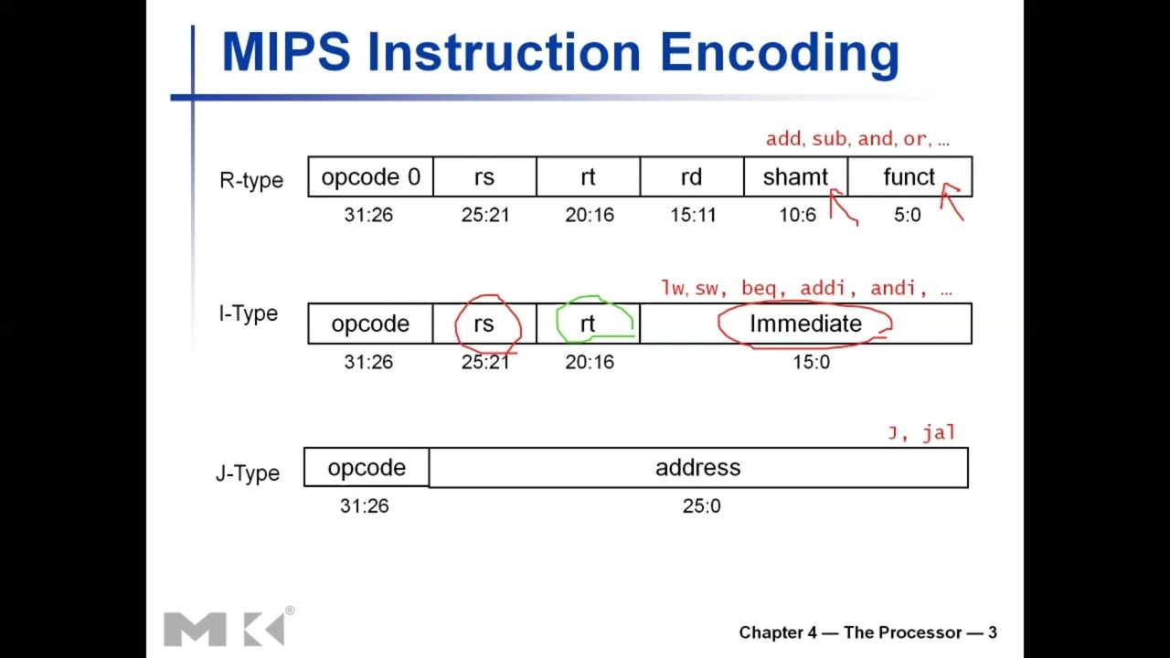
9.2.3 MIPS Instruction Encoding
Fixed 32-Bit Length
- Every instruction exactly 32 bits
- Simplifies fetch and decode
- Enables efficient pipelining
R-Type Format
[Opcode][RS][RT][RD][SHAMT][Funct]
6 bits  5   5   5    5      6 bits
Fields:
- Opcode: Always 0 for R-type
- RS: Source register 1 (5 bits for 32 registers)
- RT: Source register 2
- RD: Destination register
- SHAMT: Shift amount (for shift instructions)
- Funct: Function code (actual operation)
I-Type Format
[Opcode][RS][RT][Immediate]
6 bits  5   5   16 bits
Fields:
- Opcode: Varies by instruction
- RS: Source/base register
- RT: Source/destination register
- Immediate: 16-bit immediate value or offset
J-Type Format
[Opcode][Address]
6 bits  26 bits
Fields:
- Opcode: 2 for J, 3 for JAL
- Address: 26-bit jump target (word address)
9.3 Digital Logic Review
9.3.1 Information Encoding
Binary Representation
- Low voltage = Logic 0
- High voltage = Logic 1
- Digital signals immune to analog noise
Multi-Bit Signals
- One wire per bit
- 32-bit instruction needs 32 wires
- Parallel transmission within CPU
9.3.2 Combinational Elements
Definition
- Output is function of inputs ONLY
- No internal state or memory
- Purely functional relationship
Examples
- AND, OR, NOT gates
- Multiplexers:
Y = (S == 0) ? I0 : I1 - Adders:
Y = A + B - ALU:
Y = function(A, B, operation)
Characteristics
- Output changes immediately with input (plus propagation delay)
- Can draw complete truth table
- Asynchronous operation (no clock needed)
9.3.3 Sequential Elements (State Elements)
Definition
- Output is function of inputs AND internal state
- Has memory—stores information over time
- State persists between clock cycles
Examples
- Registers
- Flip-flops
- Register files
- Memory units
Characteristics
- Store information
- Synchronized to clock signal
- Output depends on history
9.3.4 Clocking and Timing
Clock Signal
- Periodic alternating signal: Low → High → Low → High...
- Synchronizes all sequential operations
Edge-Triggered
- Rising edge: Transition 0 → 1
- Falling edge: Transition 1 → 0
- Most processors use rising edge
Clock Period and Frequency
- Clock Period (T): Duration of one cycle
- Clock Rate (f): Cycles per second
- Relationship: $f = 1/T$
Example:
T = 250 ps = 0.25 ns
f = 1/(250 × 10^-12) = 4 GHz
9.3.5 Register Operations
Basic Register
- Stores multi-bit value (e.g., 32 bits)
- Updates on clock edge: D (input) → Q (output state)
Timing Example
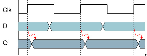
Register Timing Diagram
Register with Write Control
- Additional Write Enable signal
- Updates ONLY when clock edge AND Write Enable = 1
- Otherwise holds previous value
Timing Example
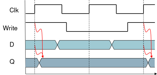
Register with Write Enable Timing Diagram
9.3.6 Critical Path and Clock Period
Combinational Logic Delay
- All combinational elements have propagation delay
- Different elements, different delays
Clock Period Constraint
- Clock Period ≥ Longest Path Delay
- Path: Register → Combinational Logic → Register
Must allow time for:
- Register output stabilization
- Combinational logic computation
- Result reaching next register input
- Setup time before next clock edge
Critical Path
- Longest delay path from register to register
- Determines minimum clock period
- Limits maximum clock frequency
Single-Cycle Constraint
- Complete one instruction per clock cycle
- Clock period must accommodate slowest instruction
- All instructions take same time (inefficient!)
9.4 CPU Execution Stages

CPU Execution Stages Overview
9.4.1 Instruction Fetch (IF)
Purpose: Retrieve next instruction from memory
Steps:
- Use Program Counter (PC) for instruction address
- Access Instruction Memory with PC
- Retrieve 32-bit instruction word
- Instruction now in CPU for processing
Hardware:
- Program Counter (32-bit register)
- Instruction Memory (read-only during execution)
- Address bus from PC to memory
- Data bus from memory to CPU
9.4.2 Instruction Decode (ID)
Purpose: Interpret instruction and extract fields
Decode Operations:
- Examine Opcode (bits 26-31):
If opcode = 0: R-type If opcode = 2 or 3: J-type Otherwise: I-type - Extract Register Numbers:
R-type: RS, RT, RD (three 5-bit fields) I-type: RS, RT (two 5-bit fields) J-type: No registers - Extract Immediate/Address:
I-type: 16-bit immediate
J-type: 26-bit address
4. Extract Function/Shift (R-type only):
Funct: bits 0-5 (ALU operation)
SHAMT: bits 6-10 (shift amount)
Control Unit Role:
- Decodes opcode
- Generates control signals
- Determines datapath activation
9.4.3 Execute (EX)
Purpose: Perform operation or calculate address
Operations by Type:
Arithmetic/Logic (R-type, I-type arithmetic):
- Send operands to ALU
- ALU performs operation
- Operation from funct field (R-type) or opcode (I-type)
Memory Access (Load/Store):
- ALU calculates address: Base + Offset
- Always performs addition
- Result is memory address
Branch:
- ALU compares registers: RS - RT
- Zero flag indicates equality
- Result determines branch decision
9.4.4 Memory Access (MEM)
Purpose: Read or write data memory
Applies To:
- Load instructions: Read from memory
- Store instructions: Write to memory
- NOT arithmetic/logic (skip this stage)
Load Operation:
- Use address from ALU
- Read data from memory
- Data will be written to register
Store Operation:
- Use address from ALU
- Get data from RT register
- Write data to memory
9.4.5 Register Write-Back (WB)
Purpose: Write result to destination register
Applies To:
- Arithmetic/Logic: Write ALU result
- Load: Write memory data
- NOT store or branch
Source Selection:
- Arithmetic/Logic: Data from ALU
- Load: Data from memory
- Multiplexer selects appropriate source
9.4.6 PC Update
Purpose: Determine next instruction address
Default: PC = PC + 4 (sequential)
Branch/Jump: PC = calculated target address
Control Flow:
- Multiplexer selects next PC value
- Sequential or branch/jump target
- Update happens at clock edge
9.5 R-Type Instruction Datapath
9.5.1 Register File
Structure:
- 32 registers (R0-R31), 32 bits each
- Three ports: 2 read, 1 write
Read Ports:
- Read Address 1: RS (5 bits)
- Read Address 2: RT (5 bits)
- Read Data 1: 32-bit output
- Read Data 2: 32-bit output
- Combinational (no clock)
Write Port:
- Write Address: RD (5 bits)
- Write Data: 32-bit input
- Write Enable: Control signal
- Synchronized (clock edge)
9.5.2 R-Type Execution Flow
Instruction: ADD $t0, $t1, $t2 (R0 = R1 + R2)
Step 1: Register Read
- Extract RS (R1) and RT (R2) fields
- Register file outputs two 32-bit values
Step 2: ALU Operation
- Inputs: Two register values
- Funct field (6 bits) → ALU control (4 bits)
- ALU performs specified operation
- Examples: ADD, SUB, AND, OR, SLT
Step 3: Write-Back
- ALU result → Register file write data
- RD field specifies destination
- Write Enable = 1
- At clock edge: Result written
9.5.3 ALU Control
Function Field Encoding:
| Funct | Operation | ALU Control |
|---|---|---|
| 0x20 | ADD | 0010 |
| 0x22 | SUB | 0110 |
| 0x24 | AND | 0000 |
| 0x25 | OR | 0001 |
| 0x2A | SLT | 0111 |
ALU Control Logic:
- Input: 6-bit funct field
- Output: 4-bit ALU operation
- Combinational logic (lookup table)
9.6 I-Type Instruction Datapath
9.6.1 Differences from R-Type
Operand Sources:
- R-type: Both from registers
- I-type: One register, one immediate
Register Usage:
- RS: Source register
- RT: Destination register (NOT source!)
- Immediate: 16-bit operand
9.6.2 Sign Extension
Problem: 16-bit immediate, 32-bit ALU
Process:
- Take 16-bit immediate
- Examine bit 15 (sign bit)
- Replicate sign bit to bits 16-31
- Result: 32-bit signed value
Examples:
16-bit: 0x0005 → 32-bit: 0x00000005 (+5)
16-bit: 0xFFFB → 32-bit: 0xFFFFFFFB (-5)
Hardware: Simple wire replication (fast)
9.6.3 Multiplexer for ALU Input
ALU Input B Selection:
- Input 0: Register data (RT) for R-type
- Input 1: Sign-extended immediate for I-type
- Select: ALUSrc control signal
ALUSrc Signal:
ALUSrc = 0: Use register (R-type, branch)
ALUSrc = 1: Use immediate (I-type)
9.7 Load/Store Instruction Datapath
9.7.1 Address Calculation
Formula: Address = Base + Offset
Components:
- Base: RS register (32-bit pointer)
- Offset: 16-bit signed immediate (sign-extended)
- ALU: Always performs addition
Examples:
LW $t1, 8($t0) # Load from $t0 + 8
SW $t2, -4($sp) # Store to $sp - 4
9.7.2 Load Word (LW)
Instruction Format:
- RS: Base register
- RT: Destination register
- Immediate: Offset
Execution:
- Read RS (base address)
- Sign-extend immediate (offset)
- ALU adds: Address = RS + offset
- Read data from memory at address
- Write data to RT register
Critical Path: Longest in single-cycle design
- Fetch → Register Read → ALU → Memory → Register Write
9.7.3 Store Word (SW)
Instruction Format:
- RS: Base register
- RT: Source register (data to store)
- Immediate: Offset
Execution:
- Read RS (base) and RT (data)
- ALU calculates address
- Write RT data to memory at address
- NO register write-back
Key Difference:
- Reads TWO registers (RS and RT)
- Memory write instead of read
- No register write stage
9.7.4 Data Memory
Interface:
- Address: From ALU (32 bits)
- Write Data: From RT register
- Read Data: To register file (for loads)
Control Signals:
- MemRead: Enable read (LW)
- MemWrite: Enable write (SW)
Multiplexer for Write-Back:
- Input 0: ALU result (arithmetic/logic)
- Input 1: Memory data (load)
- Select: MemtoReg signal
9.8 Branch Instruction Datapath
9.8.1 Branch Types
BEQ (Branch if Equal):
- Compare RS and RT
- Branch if RS == RT
BNE (Branch if Not Equal):
- Compare RS and RT
- Branch if RS != RT
9.8.2 Branch Target Calculation
Components
PC + 4: Next sequential instruction addressOffset: Sign-extended 16-bit immediate (count of instructions)Target: Computed branch destination
Target Address Formula
Target = (PC + 4) + (Offset × 4)
Explanation
- PC + 4: The PC has already advanced; branch is relative to the next instruction.
- Offset × 4: Immediate counts 32-bit words; multiply by 4 to convert to byte offset.
- Shift Left 2: Implemented by wiring (append two zero bits); no ALU operation required.
Hardware Path Summary
Immediate (16 bits) → Sign Extend (32 bits) → Shift Left 2 → Add to (PC + 4) → Branch Target
Design Notes
- No separate multiplier: shift-left achieves ×4 efficiently.
- Branch target adder runs in parallel with ALU (for comparison) in single-cycle design.
- Sign extension preserves negative offsets for backward branches.
9.8.3 Branch Execution
Step 1: Register Comparison
- Read RS and RT
- ALU subtracts: RS - RT
- Generate Zero flag
Step 2: Zero Flag Evaluation
- Zero = 1: Values equal
- Zero = 0: Values different
Step 3: Target Calculation (parallel)
- Sign-extend immediate
- Shift left 2
- Add to PC + 4
Step 4: PC Update Decision
BEQ: PCSrc = Branch AND Zero
BNE: PCSrc = Branch AND NOT(Zero)
Multiplexer:
- Input 0: PC + 4 (sequential)
- Input 1: Branch target
- Select: PCSrc
9.8.4 Sign Extension and Shifting
Sign Extension: Preserves signed offset
- Forward branch: Positive offset
- Backward branch: Negative offset
Shift Left 2: Wire routing trick
- Take bits 0-29 of sign-extended value
- Connect to bits 2-31 of result
- Append two zero wires at bits 0-1
- NO actual shifter hardware!
9.9 Complete Single-Cycle Datapath
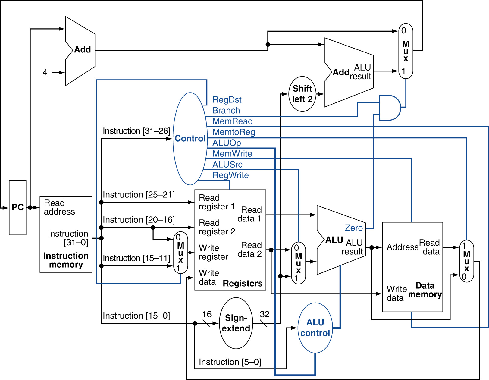
Complete Single-Cycle CPU Control and Datapath
9.9.1 Integrated Components
Instruction Fetch:
- PC register
- Instruction memory
- PC + 4 adder
Register File:
- 32 registers with 3 ports
- Two read, one write
ALU:
- Two 32-bit inputs
- Operation control
- Result output
- Zero flag
Data Memory:
- Address from ALU
- Write data from register
- Read data to register
Sign Extender:
- 16-bit input
- 32-bit output
Branch Logic:
- Target adder
- PC multiplexer
Multiplexers:
- ALU input B (register vs immediate)
- Register write data (ALU vs memory)
- Next PC (PC+4 vs branch target)
9.9.2 Control Signals
Generated by Control Unit:
1. RegDst: Register destination select
2. Branch: Branch instruction indicator
3. MemRead: Memory read enable
4. MemtoReg: Memory to register select
5. MemWrite: Memory write enable
6. ALUSrc: ALU source select
7. RegWrite: Register write enable
8. ALUOp: ALU operation type
9.9.3 Parallel Operations
Key Insight: Hardware operates in PARALLEL
- All datapath elements active simultaneously
- Some produce meaningless results
- Control signals select valid paths
Example: R-type instruction
- Sign extender operates on bits 0-15
- Produces meaningless output (no immediate in R-type)
- Multiplexer doesn't select it (ALUSrc = 0)
9.9.4 Critical Path Analysis
Path for Load Word (longest):
1. Instruction fetch:     200 ps
2. Register read:         150 ps
3. Sign extend:           50 ps
4. Multiplexer:           25 ps
5. ALU address calc:      200 ps
6. Data memory access:    200 ps
7. Multiplexer:           25 ps
8. Register write setup:  100 ps
Total:                    950 ps
Clock Period: Must be ≥ 950 ps
Max Frequency: 1/950 ps ≈ 1.05 GHz
Inefficiency:
- ALL instructions take 950 ps
- Fast R-type (650 ps) waits
- Wasted time per fast instruction
9.9.5 Single-Cycle Disadvantages
Inefficiency:
- Fast instructions wait for slow ones
- Clock period by worst case
- Cannot optimize common case
Hardware Duplication:
- Separate instruction/data memories
- Multiple adders
- Cannot reuse hardware in same cycle
No Parallelism:
- One instruction at a time
- Hardware mostly idle
- Poor resource utilization
Advantages:
- Simple design
- Simple control
- One instruction per cycle (conceptually)
- Good for learning
Key Takeaways
- Microarchitecture is hardware implementation of ISA - translating instruction semantics to hardware operations.
- MIPS uses three instruction types: R-type (registers), I-type (immediate), J-type (jump).
- Fixed 32-bit instructions simplify fetch/decode and enable efficient pipelining.
- Combinational elements have output as function of inputs only; sequential elements have state.
- Clock period must exceed longest combinational path between sequential elements.
- Six execution stages: Fetch, Decode, Execute, Memory, Write-back, PC Update.
- Register file has three ports: two read (combinational), one write (clocked).
- Sign extension converts 16-bit immediate to 32-bit preserving signed value.
- Multiplexers select between data sources based on control signals.
- ALU operations vary by instruction: addition (load/store), subtraction (branch), varies (R-type).
- Critical path determines clock period - load word is longest in single-cycle design.
- Single-cycle processor completes one instruction per cycle but inefficiently (all take same time).
- Separate instruction and data memories required for single-cycle (both accessed same cycle).
- Control signals orchestrate datapath - generated by control unit from opcode.
- All hardware operates in parallel - control signals select valid results, ignore others.
Summary
Microarchitecture bridges the gap between software instructions and hardware implementation, revealing how processors execute programs. Building a single-cycle MIPS processor requires understanding digital logic fundamentals, datapath component design, and control signal generation. While conceptually simple (one instruction per cycle), the single-cycle design is inefficient because all instructions must complete within the time required by the slowest instruction. The critical path—typically the load word instruction—determines the maximum clock frequency. Understanding this foundation prepares us for more sophisticated designs including multi-cycle processors (which break execution into multiple stages) and pipelined processors (which overlap instruction execution for higher throughput). These microarchitecture concepts apply broadly across processor design, from embedded systems to high-performance superscalar processors.