Click the thumbnail above to watch the video lecture on YouTube
10.1 Introduction
This lecture completes the single-cycle MIPS processor design by exploring the control unit—the component that generates control signals based on instruction opcodes. We examine ALU control generation using a two-stage approach, design the main control unit, analyze control signal purposes, and create truth tables mapping instructions to control patterns. Understanding control unit design reveals how hardware interprets instructions and orchestrates datapath operations, completing our understanding of processor implementation.
10.2 Control Unit Overview
10.2.1 Recap of Datapath Components
Previously Covered:
- Register File (32 registers, 3 ports)
- ALU (arithmetic/logic operations)
- Instruction Memory (stores program)
- Data Memory (stores data)
- Adders (PC+4, branch target)
- Multiplexers (data source selection)
- Sign Extender (16-bit to 32-bit)
- Shifter (branch offset left 2)
10.2.2 Control Unit Purpose
Function: Generate control signals based on instruction
Inputs:
- Opcode (bits 26-31, 6 bits)
- Funct field (bits 0-5, 6 bits) for R-type
Outputs: Control signals for datapath
- Multiplexer selections
- Register write enable
- Memory read/write
- ALU operation
- Branch decision
10.2.3 Instruction Subset for Study
Selected Instructions:
- Load Word (LW): Memory read
- Store Word (SW): Memory write
- Branch if Equal (BEQ): Conditional branch
- R-type: Arithmetic, logic, shift
Coverage:
- Uses almost all datapath hardware
- Representative of most control signals
- Excludes: Jump instructions, I-type arithmetic
10.3 ALU Operations for Different Instructions
10.3.1 Load/Store Instructions
Address Calculation:
Address = Base Register + Immediate Offset
         = RS + Sign_Extend(Immediate)
ALU Function: ADDITION (always)
- Input A: RS register value
- Input B: Sign-extended immediate
- Operation: ADD
- ALU Control: 0010 (binary)
- Result: Memory address
Example:
LW $t1, 8($t0)    # Address = $t0 + 8
SW $t2, -4($sp)   # Address = $sp + (-4)
10.3.2 Branch Instructions
Comparison Operation:
Compare RS and RT for equality
Method: Subtract RT from RS
ALU Function: SUBTRACTION
- Input A: RS register value
- Input B: RT register value
- Operation: SUB
- ALU Control: 0110 (binary)
- Result: RS - RT
- Zero Flag: Indicates if result is zero (equal)
Branch Decision:
Zero = 1: RS == RT, take branch
Zero = 0: RS != RT, don't take branch
10.3.3 R-Type Instructions
Variable Operations: Determined by funct field
ALU Function: DEPENDS ON FUNCT
- Input A: RS register value
- Input B: RT register value
- Operation: From funct field
- ALU Control: Varies
- Result: Written to RD register
Funct Field Mapping:
| Funct | Operation | ALU Control |
|---|---|---|
| 0x20 | ADD | 0010 |
| 0x22 | SUB | 0110 |
| 0x24 | AND | 0000 |
| 0x25 | OR | 0001 |
| 0x2A | SLT | 0111 |
10.4 ALU Control Signal
10.4.1 Signal Format
4-Bit Signal: Specifies ALU operation
Possible Operations (2⁴ = 16):
0000: AND
0001: OR
0010: ADD
0110: SUBTRACT
0111: Set on Less Than (SLT)
1100: NOR
Usage:
- Not all 16 combinations used
- Could use 3 bits for 8 operations
- 4-bit standard allows expansion
10.4.2 Control Signal Usage by Instruction
Load/Store:
- ALU Control = 0010 (ADD)
- Fixed operation
- Independent of instruction specifics
Branch:
- ALU Control = 0110 (SUBTRACT)
- Fixed operation
- Zero flag is critical output
R-Type:
- ALU Control = Varies
- Must decode funct field
- Different operations need different controls
10.5 Two-Stage ALU Control Generation
10.5.1 Design Rationale
Why Two Stages?
Efficiency:
- Some instructions don't need funct field
- Separates opcode-level from operation-level
- Faster for non-R-type instructions
Timing Optimization:
- Other control signals needed faster
- Examples: Register addressing, immediate routing
- ALU control can afford slight delay
Modularity:
- Stage 1: Main control (opcode-based)
- Stage 2: ALU control (operation-specific)
- Cleaner design separation
10.5.2 Stage 1: Generate ALUOp
Input: Opcode (6 bits)
Output: ALUOp (2 bits)
Encoding:
| Instruction | Opcode | ALUOp |
|---|---|---|
| Load Word | 100011 | 00 |
| Store Word | 101011 | 00 |
| Branch Equal | 000100 | 01 |
| R-type | 000000 | 10 |
ALUOp Meaning:
- 00: Perform ADD (address calculation)
- 01: Perform SUBTRACT (comparison)
- 10: Operation from funct field
Logic: Purely combinational based on opcode
10.5.3 Stage 2: Generate ALU Control
Inputs:
- ALUOp (2 bits from Stage 1)
- Funct field (6 bits from instruction)
- Total: 8 input bits
Output: ALU Control (4 bits)
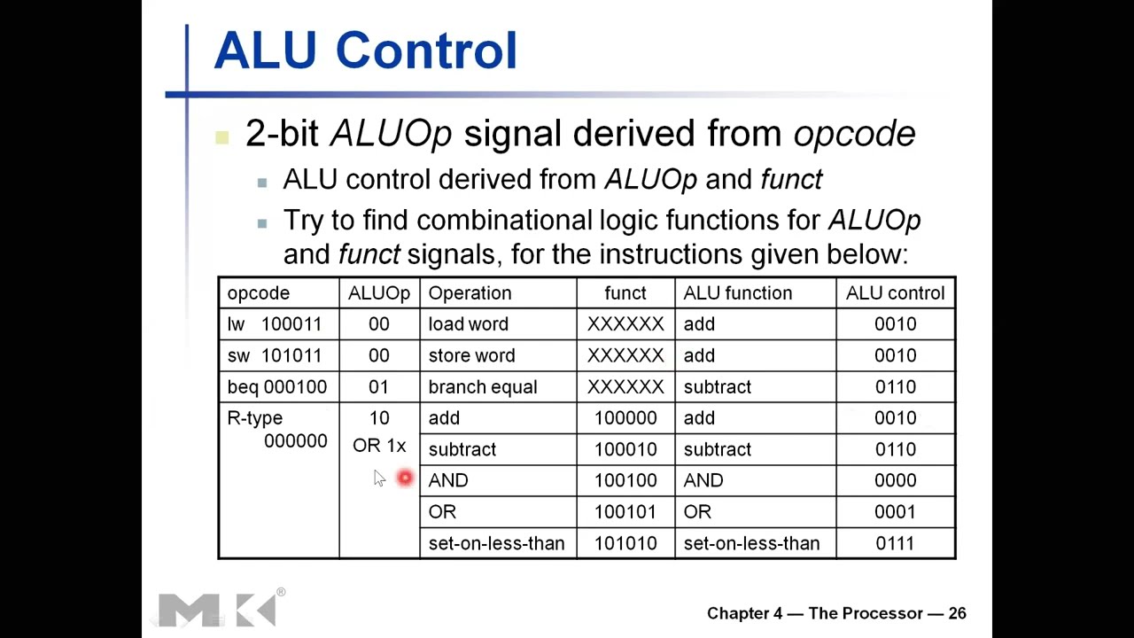
Truth Table:
| ALUOp | Funct | ALU Control | Operation |
|---|---|---|---|
| 00 | XXXXXX | 0010 | ADD (LW/SW) |
| 01 | XXXXXX | 0110 | SUB (BEQ) |
| 10 | 100000 | 0010 | ADD (R-type) |
| 10 | 100010 | 0110 | SUB (R-type) |
| 10 | 100100 | 0000 | AND |
| 10 | 100101 | 0001 | OR |
| 10 | 101010 | 0111 | SLT |
"X" Notation: Don't Care
- For ALUOp = 00 or 01, funct irrelevant
- Simplifies logic design
- Reduces gate count
10.5.4 Complete ALU Control Path
Flow Diagram:
Instruction Opcode (6 bits)
         ↓
  [Main Control Unit]
         ↓
   ALUOp (2 bits)  +  Funct Field (6 bits)
         ↓                    ↓
         └──────────┬─────────┘
                    ↓
         [ALU Control Unit]
                    ↓
          ALU Control (4 bits)
                    ↓
                  [ALU]
Advantages:
- Modular design
- Simplified main control
- Localized R-type complexity
- Easier to verify
10.6 Main Control Signals
10.6.1 Complete Signal List
Signals Generated:
- RegDst (1 bit): Register destination select
- Branch (1 bit): Branch instruction indicator
- MemRead (1 bit): Memory read enable
- MemtoReg (1 bit): Memory to register select
- MemWrite (1 bit): Memory write enable
- ALUSrc (1 bit): ALU source select
- RegWrite (1 bit): Register write enable
- ALUOp (2 bits): To ALU control unit
Total: 9 control bits from main control
10.6.2 RegDst (Register Destination)
Purpose: Select which field specifies write destination
Multiplexer Control:
- Input 0: RT field (bits 16-20)
- Input 1: RD field (bits 11-15)
- Output: Register write address (5 bits)
Settings:
RegDst = 0: Write to RT (Load Word)
RegDst = 1: Write to RD (R-type)
Rationale:
- Load Word: RT is destination (I-type format)
- R-type: RD is destination (R-type format)
- Store/Branch: Don't care (no write)
Examples:
LW $t1, 8($t0)     # Write to $t1 (RT) → RegDst = 0
ADD $t2, $t3, $t4  # Write to $t2 (RD) → RegDst = 1
10.6.3 Branch
Purpose: Indicate if instruction is branch
Usage: Combined with Zero flag for PC selection
Settings:
Branch = 0: Not a branch (LW, SW, R-type)
Branch = 1: Branch instruction (BEQ, BNE)
PC Selection Logic:
For BEQ:
PCSrc = Branch AND Zero
(Take branch if instruction is branch AND comparison equal)
For BNE:
PCSrc = Branch AND NOT(Zero)
(Take branch if instruction is branch AND comparison not equal)
10.6.4 MemRead
Purpose: Enable reading from data memory
Settings:
MemRead = 0: No memory read (R-type, SW, BEQ)
MemRead = 1: Read from memory (LW)
Function:
- Controls data memory read enable
- When high: Memory outputs data
- When low: Memory read inactive
10.6.5 MemtoReg (Memory to Register)
Purpose: Select source of register write data
Multiplexer Control:
- Input 0: ALU result
- Input 1: Data memory read data
- Output: Register write data (32 bits)
Settings:
MemtoReg = 0: Write ALU result (R-type)
MemtoReg = 1: Write memory data (LW)
Examples:
ADD $t1, $t2, $t3  # $t1 = ALU result → MemtoReg = 0
LW $t1, 8($t0)     # $t1 = memory data → MemtoReg = 1
10.6.6 MemWrite
Purpose: Enable writing to data memory
Settings:
MemWrite = 0: No memory write (R-type, LW, BEQ)
MemWrite = 1: Write to memory (SW)
Function:
- Controls data memory write enable
- When high: Data written (on clock edge)
- When low: Memory write disabled
10.6.7 ALUSrc (ALU Source)
Purpose: Select second ALU operand source
Multiplexer Control:
- Input 0: Register file Read Data 2 (RT value)
- Input 1: Sign-extended immediate
- Output: ALU Input B (32 bits)
Settings:
ALUSrc = 0: Use register (R-type, BEQ)
ALUSrc = 1: Use immediate (LW, SW)
Examples:
ADD $t1, $t2, $t3  # Use $t3 → ALUSrc = 0
LW $t1, 8($t0)     # Use imm 8 → ALUSrc = 1
10.6.8 RegWrite
Purpose: Enable writing to register file
Settings:
RegWrite = 0: No register write (SW, BEQ)
RegWrite = 1: Write to register (R-type, LW)
Usage by Instruction:
R-type:    RegWrite = 1 (write ALU result)
Load Word: RegWrite = 1 (write memory data)
Store Word: RegWrite = 0 (no write)
Branch:    RegWrite = 0 (no write)
10.7 Control Signal Truth Table
10.7.1 Complete Table
| Instruction | RegDst | ALUSrc | MemtoReg | RegWrite | MemRead | MemWrite | Branch | ALUOp |
|---|---|---|---|---|---|---|---|---|
| R-type | 1 | 0 | 0 | 1 | 0 | 0 | 0 | 10 |
| Load Word | 0 | 1 | 1 | 1 | 1 | 0 | 0 | 00 |
| Store Word | X | 1 | X | 0 | 0 | 1 | 0 | 00 |
| Branch Eq | X | 0 | X | 0 | 0 | 0 | 1 | 01 |
Legend:
- 0: Signal low/false/select input 0
- 1: Signal high/true/select input 1
- X: Don't Care (not used, can be anything)
10.7.2 R-Type Control
Settings:
RegDst = 1:     Write to RD field
ALUSrc = 0:     Second operand from register (RT)
MemtoReg = 0:   Write ALU result
RegWrite = 1:   Enable register write
MemRead = 0:    No memory read
MemWrite = 0:   No memory write
Branch = 0:     Not a branch
ALUOp = 10:     Consult funct field
Active Elements:
- Instruction fetch
- Register file (read RS, RT; write RD)
- ALU (operation from funct)
- Register write from ALU
- PC updated to PC + 4
Inactive Elements:
- Data memory (not accessed)
- Branch target (computed but not used)
- Sign extender (operates but ignored)
10.7.3 Load Word Control
Settings:
RegDst = 0:     Write to RT field
ALUSrc = 1:     Second operand from immediate
MemtoReg = 1:   Write memory data
RegWrite = 1:   Enable register write
MemRead = 1:    Enable memory read
MemWrite = 0:   No memory write
Branch = 0:     Not a branch
ALUOp = 00:     ALU performs ADD
Active Elements:
- Instruction fetch
- Register file (read RS; write RT)
- Sign extender
- ALU (ADD for address)
- Data memory (read)
- Register write from memory
- PC updated to PC + 4
Critical Path: Longest delay
- Fetch → Reg Read → Sign Extend → ALU → Memory → Reg Write
10.7.4 Store Word Control
Settings:
RegDst = X:     Don't care (no register write)
ALUSrc = 1:     Second operand from immediate
MemtoReg = X:   Don't care (no register write)
RegWrite = 0:   No register write
MemRead = 0:    No memory read
MemWrite = 1:   Enable memory write
Branch = 0:     Not a branch
ALUOp = 00:     ALU performs ADD
Key Difference from Load:
- Read TWO registers (RS for base, RT for data)
- Memory write instead of read
- No register write stage
10.7.5 Branch if Equal Control
Settings:
RegDst = X:     Don't care (no register write)
ALUSrc = 0:     Second operand from register (RT)
MemtoReg = X:   Don't care (no register write)
RegWrite = 0:   No register write
MemRead = 0:    No memory read
MemWrite = 0:   No memory write
Branch = 1:     This is a branch
ALUOp = 01:     ALU performs SUBTRACT
Active Elements:
- Instruction fetch
- Register file (read RS, RT)
- ALU (SUBTRACT for comparison, Zero flag)
- Sign extender + shift (branch target)
- Branch target adder (PC + 4 + offset)
- PC multiplexer (select based on Branch AND Zero)
Branch Decision Logic:
Zero = (RS - RT == 0)
PCSrc = Branch AND Zero
If PCSrc:
    PC = Branch Target
Else:
    PC = PC + 4
10.8 Control Unit Implementation
10.8.1 Input to Control Unit
Primary Input: Opcode (bits 26-31, 6 bits)
- Identifies instruction type
- Determines all control signal values
Secondary Input: Funct field (bits 0-5, 6 bits)
- Only for R-type (opcode = 000000)
- Specifies ALU operation
10.8.2 Combinational Logic Design
Method: Standard digital logic techniques
Steps:
- Create truth table (opcode → control signals)
- List all control signals as outputs
- Fill in values for each instruction
- Use Karnaugh maps or Boolean algebra to minimize
- Implement with logic gates
Example for RegWrite:
RegWrite = (R-type) OR (Load Word)
RegWrite = (opcode == 000000) OR (opcode == 100011)
10.8.3 Control Unit Structure
ROM-Based Implementation:
- Opcode as ROM address
- ROM location stores control pattern
- Simple but inflexible
PLA (Programmable Logic Array):
- Implements minimized logic equations
- More efficient than ROM
- Standard for simple processors
Hardwired Logic:
- Custom logic gates
- Fastest implementation
- Most common for high-performance
Microcode (not typical for RISC):
- Control signals stored in memory
- More flexible but slower
- Used in CISC (e.g., x86)
10.8.4 Timing Considerations
Signal Generation Time:
- Must complete early in clock cycle
- Before datapath elements need signals
- Critical for clock frequency
Signal Stability:
- Must remain stable throughout cycle
- Changes only between instructions
- Combinational logic ensures this
Clock Period Impact:
- Control logic adds delay
- Typically small vs. ALU/memory
- Well-designed control has minimal impact
10.9 Why Separate MemRead and MemWrite?
10.9.1 Initial Observation
Question: Seem mutually exclusive—why not one signal?
- Could use: 0 = Read, 1 = Write
- Appears redundant
10.9.2 Answer: Yes, Separate Signals Needed
Timing Control:
- Write Enable: Specifies WHEN to write
- Read Enable: Specifies WHEN valid data available
- Different timing requirements
No Operation State:
- Both = 0: No memory access
- Common for R-type and branch
- Single signal couldn't represent this
Three States Required:
MemRead=1, MemWrite=0: Read
MemRead=0, MemWrite=1: Write
MemRead=0, MemWrite=0: No access
(MemRead=1, MemWrite=1: Invalid)
10.9.3 Future: Pipelined Processors
Concurrent Access:
- Different pipeline stages access memory
- One stage reading, another writing
- Separate signals essential
Memory Banking:
- Separate read/write ports
- Enables simultaneous access
- Separate signals control independent ports
10.9.4 Design Philosophy
Orthogonality:
- Each signal controls independent function
- Easier to understand and verify
- Reduces design errors
Flexibility:
- Supports future enhancements
- Allows memory optimization
- Standard practice
10.10 Complete Datapath with Control
10.10.1 Integrated System
Components Connected:
- Control Unit (generates signals)
- Datapath (executes operations)
- Blue lines: Control signals
- Black lines: Data paths
Control Unit Connections:
- Input: Instruction opcode
- Outputs: All control signals
- Fan out to datapath elements
ALU Control Unit:
- Separate box near ALU
- Inputs: ALUOp, Funct
- Output: ALU Control (4 bits)
10.10.2 Example: Load Word Execution
Instruction: LW $t1, 8($t0)
Step 1: Fetch
PC → Instruction Memory
Opcode = 100011 (LW)
Step 2: Control Signals
RegDst=0, ALUSrc=1, MemtoReg=1, RegWrite=1,
MemRead=1, MemWrite=0, Branch=0, ALUOp=00
Step 3: Register Read
RS field ($t0) → Register file
Read Data 1 = $t0 value
Step 4: ALU
Immediate = 8
Sign-extended to 32 bits
ALUSrc=1: Selects immediate
ALU performs ADD: $t0 + 8 = address
Step 5: Memory
MemRead=1: Memory reads at address
Data output from memory
Step 6: Write-Back
MemtoReg=1: Selects memory data
RegDst=0: Selects RT ($t1)
RegWrite=1: Enables write
At clock edge: Memory data → $t1
Step 7: PC Update
Branch=0: PCSrc=0
PC updated to PC + 4
Key Takeaways
- Control unit generates signals based on instruction opcode, orchestrating datapath operations.
- ALU control uses two-stage generation: Opcode → ALUOp (2 bits) → ALU Control (4 bits).
- Stage 1 (Main Control): Opcode to ALUOp - identifies operation category.
- Stage 2 (ALU Control): ALUOp + Funct to ALU Control - specifies exact operation.
- Two-stage design optimizes timing and modularity, separating concerns.
- Main control signals: RegDst, Branch, MemRead, MemtoReg, MemWrite, ALUSrc, RegWrite, ALUOp.
- Load/Store always use ADD for address calculation, regardless of other details.
- Branch uses SUBTRACT for comparison, with Zero flag indicating equality.
- R-type ALU operation from funct field, providing operation flexibility.
- Instruction format regularity simplifies control, with consistent field positions.
- Register roles vary by instruction type, especially RT (destination vs. source).
- Control signals mutually exclusive for proper operation - only valid combinations used.
- Separate MemRead/MemWrite needed for no-op state and future pipelining.
- Control logic is combinational (no state), generating signals each cycle.
- Truth tables map opcode to control patterns, enabling systematic design.
- "Don't care" values simplify logic minimization, reducing gate count.
- Control unit design uses standard digital logic techniques, including K-maps and Boolean algebra.
- Datapath elements may operate but outputs ignored if not selected by control signals.
- Complete processor integrates datapath and control, with control signals orchestrating all operations.
- Single-cycle design simple but inefficient - foundation for advanced multi-cycle and pipelined designs.
Summary
The control unit completes the single-cycle MIPS processor, generating control signals that orchestrate datapath operations based on instruction opcodes. The two-stage ALU control generation (opcode → ALUOp → ALU Control) elegantly separates concerns, with the main control handling instruction-level decisions and the ALU control handling operation-specific details. Each control signal serves a specific purpose, from selecting multiplexer inputs (RegDst, ALUSrc, MemtoReg) to enabling register and memory operations (RegWrite, MemRead, MemWrite) to handling branches (Branch). Truth tables systematically map instructions to control patterns, with "don't care" values simplifying logic design. While the single-cycle processor provides conceptual clarity and simplicity, its inefficiency (all instructions taking the same time as the slowest) motivates more sophisticated designs. Understanding this foundation prepares us for multi-cycle processors (which break execution into variable-length stages) and pipelined processors (which overlap instruction execution for higher throughput), both building on the control principles established here.