Click the thumbnail above to watch the video lecture on YouTube
11.1 Introduction
This lecture completes the single-cycle MIPS processor design by providing comprehensive analysis of control signals for all instruction types (R-type, Branch, Load, Store, Jump), introducing detailed timing analysis with concrete delay values, and demonstrating the fundamental performance limitations that motivate the evolution toward multi-cycle and pipelined implementations. We build upon previous datapath and control unit knowledge to create a functioning processor while understanding why single-cycle design, though conceptually simple, proves inefficient in practice.
11.2 Lecture Overview and Context
11.2.1 Recap from Previous Lectures
The foundational work completed in previous lectures includes:
Completed Topics:
- Datapath components: Register file, ALU, memories, adders, multiplexers
- Sign extension and shifting for immediate operands
- Control unit concept and ALU control generation
- Control signal purposes and functions
Current Focus:
- Complete control signal analysis for all instructions
- Detailed walkthrough of instruction execution
- Jump instruction integration
- Timing analysis with concrete delay values
- Performance limitations of single-cycle design
11.2.2 Instruction Subset Review
Selected Instructions for Study:
- R-type: ADD, SUB, AND, OR (arithmetic/logic operations)
- Load Word (LW): Memory read
- Store Word (SW): Memory write
- Branch if Equal (BEQ): Conditional branch
- Jump (J): Unconditional jump
Coverage:
- Represents 95% of MIPS microarchitecture hardware
- Comprehensive enough for understanding design principles
- Omits some I-type arithmetic (covered conceptually)
- Foundation for complete processor understanding
11.3 Control Unit Inputs and Outputs
11.3.1 Control Unit Inputs
Total Input Bits: 12 bitsPrimary Input - Opcode (6 bits):
- Bits 26-31 of instruction
- Identifies instruction type
- Used for almost all control signal generation
- Most significant determinant of control behavior
Secondary Input - Funct Field (6 bits):
- Bits 0-5 of instruction
- Only relevant for R-type instructions (opcode = 000000)
- Specifies ALU operation for R-type
- Ignored for I-type and J-type instructions
Usage Pattern:
- Opcode always examined
- Funct field examined only when opcode = 0 (R-type)
- Combined with ALUOp for final ALU control signal
11.3.2 Control Unit Outputs
Total Output Bits: 9 bits (8 signals, one is 2-bit)Control Signals Generated:
- RegDst (1 bit): Select register write address
- Branch (1 bit): Instruction is branch type
- MemRead (1 bit): Enable memory read
- MemtoReg (1 bit): Select register write data source
- MemWrite (1 bit): Enable memory write
- ALUSrc (1 bit): Select ALU second operand source
- RegWrite (1 bit): Enable register file write
- ALUOp (2 bits): ALU operation category
Additional Signal for Jump:
- Jump (1 bit): Select jump target for PC
Implementation:
- Combinational logic circuit
- Inputs: Opcode and Funct field
- Outputs: Control signals
- Design method: Truth tables, Karnaugh maps, Boolean minimization
- To be implemented in Lab 5
11.4 R-Type Instruction Detailed Analysis
11.4.1 Instruction Format
Encoding Structure (32 bits):
- Bits 26-31: Opcode = 000000 (0) - ALL R-type instructions
- Bits 21-25: RS (5 bits) - First source register
- Bits 16-20: RT (5 bits) - Second source register
- Bits 11-15: RD (5 bits) - Destination register
- Bits 6-10: SHAMT (5 bits) - Shift amount
- Bits 0-5: Funct (6 bits) - Function code (specifies operation)
Example: ADD $1, $2, $3
Encoding: 000000 00010 00011 00001 00000 100000
         |Opcode| RS | RT | RD |SHAMT| Funct |
         |   0  |  2 |  3 |  1 |  0  |  32   |
Operation: $1 = $2 + $3
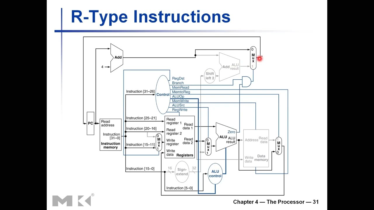
11.4.2 Datapath Elements Used
R-Type Instruction Datapath
Active Elements (shown in black):
- Instruction Memory: Fetch instruction
- Program Counter: Current instruction address
- PC + 4 Adder: Calculate next sequential address
- Register File: Read RS, RT; Write RD
- Multiplexer (RegDst): Select RD as write address
- Multiplexer (ALUSrc): Select RT value (not immediate)
- ALU: Perform operation specified by funct
- Multiplexer (MemtoReg): Select ALU result (not memory)
- Multiplexer (PC source): Select PC+4 (not branch)
Inactive Elements (grayed out):
- Data Memory: Not accessed
- Sign Extender: Not used (no immediate value)
- Branch Target Adder: Calculated but not used
- Shift Left 2: Not used
11.4.3 Control Signal Values for R-Type
Exercise Example: ADD $1, $2, $3
| Signal | Value | Reason |
|---|---|---|
| RegDst | 1 | Write to RD (bits 11-15), not RT |
| Branch | 0 | Not a branch instruction |
| MemRead | 0 | Not reading from memory |
| MemtoReg | 0 | Write ALU result (not memory data) |
| ALUOp | 10 | R-type: Consult funct field |
| MemWrite | 0 | Not writing to memory |
| ALUSrc | 0 | Second operand from register RT (not immediate) |
| RegWrite | 1 | Write result to destination register |
Detailed Explanations:
RegDst = 1:
- Multiplexer selects input 1
- Input 1: Bits 11-15 (RD field)
- Input 0: Bits 16-20 (RT field)
- R-type destination always in RD
Branch = 0:
- Not a branch instruction
- Branch control AND Zero → 0 AND X = 0
- PC source multiplexer selects PC+4
MemRead = 0, MemWrite = 0:
- R-type doesn't access data memory
- Memory control signals disabled
- Data memory outputs ignored (don't care)
MemtoReg = 0:
- Multiplexer selects ALU result
- Not memory data (memory not accessed)
- ALU result goes to register write data
ALUOp = 10 (binary):
- Indicates R-type instruction
- ALU Control Unit examines funct field
- For ADD: funct = 100000 → ALU Control = 0010 (ADD)
ALUSrc = 0:
- Multiplexer selects register value
- Register file Read Data 2 (RT value)
- Not sign-extended immediate
RegWrite = 1:
- Enable register file write
- Result written to RD at clock edge
- Essential for saving computation result
11.4.4 Execution Steps for R-Type
Step 1: Instruction Fetch
- PC value → Instruction Memory address
- Instruction word retrieved
- Opcode (000000) sent to Control Unit
Step 2: Control Signal Generation
- Control Unit decodes opcode = 0
- Identifies R-type instruction
- Generates all control signals
- Sends funct field to ALU Control
Step 3: Register Read
- RS field (00010 = 2) → Read Address 1
- RT field (00011 = 3) → Read Address 2
- Read Data 1 = $2 value
- Read Data 2 = $3 value
Step 4: ALU Operation
- ALUSrc = 0: Select RT value for Input B
- Input A = $2 value, Input B = $3 value
- ALU Control = 0010 (ADD operation)
- ALU Result = $2 + $3
Step 5: Register Write Preparation
- MemtoReg = 0: Select ALU result
- RegDst = 1: Select RD (00001 = 1)
- Write Data = ALU result
- Write Address = $1
Step 6: Clock Edge Actions
- RegWrite = 1 enabled
- ALU result written to $1
- PC updated to PC + 4
- Next instruction fetch begins
11.5 Branch If Equal Instruction Detailed Analysis
11.5.1 Instruction Format
Encoding Structure (32 bits):
- Bits 26-31: Opcode = 000100 (4) - BEQ
- Bits 21-25: RS (5 bits) - First comparison register
- Bits 16-20: RT (5 bits) - Second comparison register
- Bits 0-15: Immediate (16 bits) - Branch offset (in instructions)
Example: BEQ $1, $2, 100
Encoding: 000100 00001 00010 0000000001100100
         |Opcode|  RS  |  RT  |    Immediate    |
         |   4  |   1  |   2  |       100       |
Operation: If ($1 == $2) then PC = PC + 4 + (100 × 4)
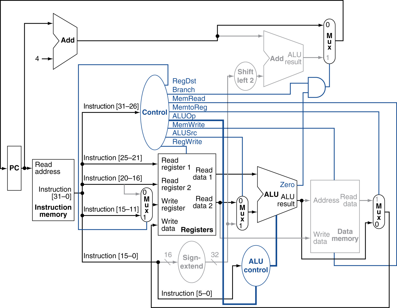
11.5.2 Datapath Elements Used
Branch If Equal Instruction Datapath
Active Elements:
- Instruction Memory: Fetch instruction
- Program Counter & PC+4 Adder
- Register File: Read RS, RT (no write)
- ALU: Subtract RT from RS
- Zero Flag: Compare result to zero
- Sign Extender: Extend 16-bit offset to 32-bit
- Shift Left 2: Convert word offset to byte offset
- Branch Target Adder: Calculate PC + 4 + (offset × 4)
- AND Gate: Combine Branch signal and Zero flag
- PC Source Multiplexer: Select next PC value
Inactive Elements:
- Data Memory: Not accessed
- Register Write: Not writing to registers
- ALU Result (except Zero flag): Not used
11.5.3 Control Signal Values for BEQ
Exercise Example: BEQ $1, $2, 100
| Signal | Value | Reason |
|---|---|---|
| RegDst | X | Don't care (not writing to register) |
| Branch | 1 | This IS a branch instruction |
| MemRead | 0 | Not reading from memory |
| MemtoReg | X | Don't care (not writing to register) |
| ALUOp | 01 | Perform SUBTRACT for comparison |
| MemWrite | 0 | Not writing to memory |
| ALUSrc | 0 | Compare two register values (not immediate) |
| RegWrite | 0 | Not writing to register file |
Detailed Explanations:
RegDst = X (Don't Care):
- RegWrite = 0, so write address irrelevant
- No register write operation
- Multiplexer output ignored
- Using X simplifies Boolean logic
Branch = 1:
- Identifies instruction as branch type
- Feeds into AND gate with Zero flag
- PCSrc = Branch AND Zero
- If Zero = 1 (values equal): Take branch
- If Zero = 0 (values differ): Don't take branch
MemRead = 0, MemWrite = 0:
- Branch doesn't access memory
- Memory control signals disabled
MemtoReg = X (Don't Care):
- RegWrite = 0, so write data source irrelevant
- Multiplexer output ignored
ALUOp = 01:
- Specifies SUBTRACT operation
- ALU Control receives 01
- Generates ALU Control = 0110 (SUB)
- Independent of funct field
ALUSrc = 0:
- Need RT value from register (not immediate)
- Immediate used for branch target (not ALU input)
- ALU compares RS and RT register values
RegWrite = 0:
- Branch doesn't modify registers
- Essential to prevent accidental writes
- If =1, would corrupt register file
11.5.4 Branch Target Calculation
Word Offset to Byte Offset:
- Immediate field: 100 (in instructions/words)
- Sign extend to 32 bits: 0x00000064
- Shift left by 2: 0x00000190 (multiply by 4)
- Result: 400 bytes (100 instructions × 4 bytes/instruction)
Branch Target Address:
- Current PC + 4: Address of next sequential instruction
- Offset: 400 bytes
- Branch Target = (PC + 4) + 400
Example:
- Current instruction at address 1000
- PC + 4 = 1004
- Branch Target = 1004 + 400 = 1404
- If branch taken: Next instruction at 1404
- If branch not taken: Next instruction at 1004
PCSrc Selection:
PCSrc = Branch AND Zero
      = 1 AND (RS == RT ? 1 : 0)

If PCSrc = 1: PC ← Branch Target (1404)
If PCSrc = 0: PC ← PC + 4 (1004)
11.6 Load Word Instruction Detailed Analysis
11.6.1 Instruction Format
Encoding Structure (32 bits):
- Bits 26-31: Opcode = 100011 (35) - LW
- Bits 21-25: RS (5 bits) - Base address register
- Bits 16-20: RT (5 bits) - Destination register
- Bits 0-15: Immediate (16 bits) - Address offset
Example: LW $8, 32($9)
Encoding: 100011 01001 01000 0000000000100000
         |Opcode|  RS  |  RT  |    Immediate    |
         |  35  |   9  |   8  |       32        |
Operation: $8 = Memory[$9 + 32]
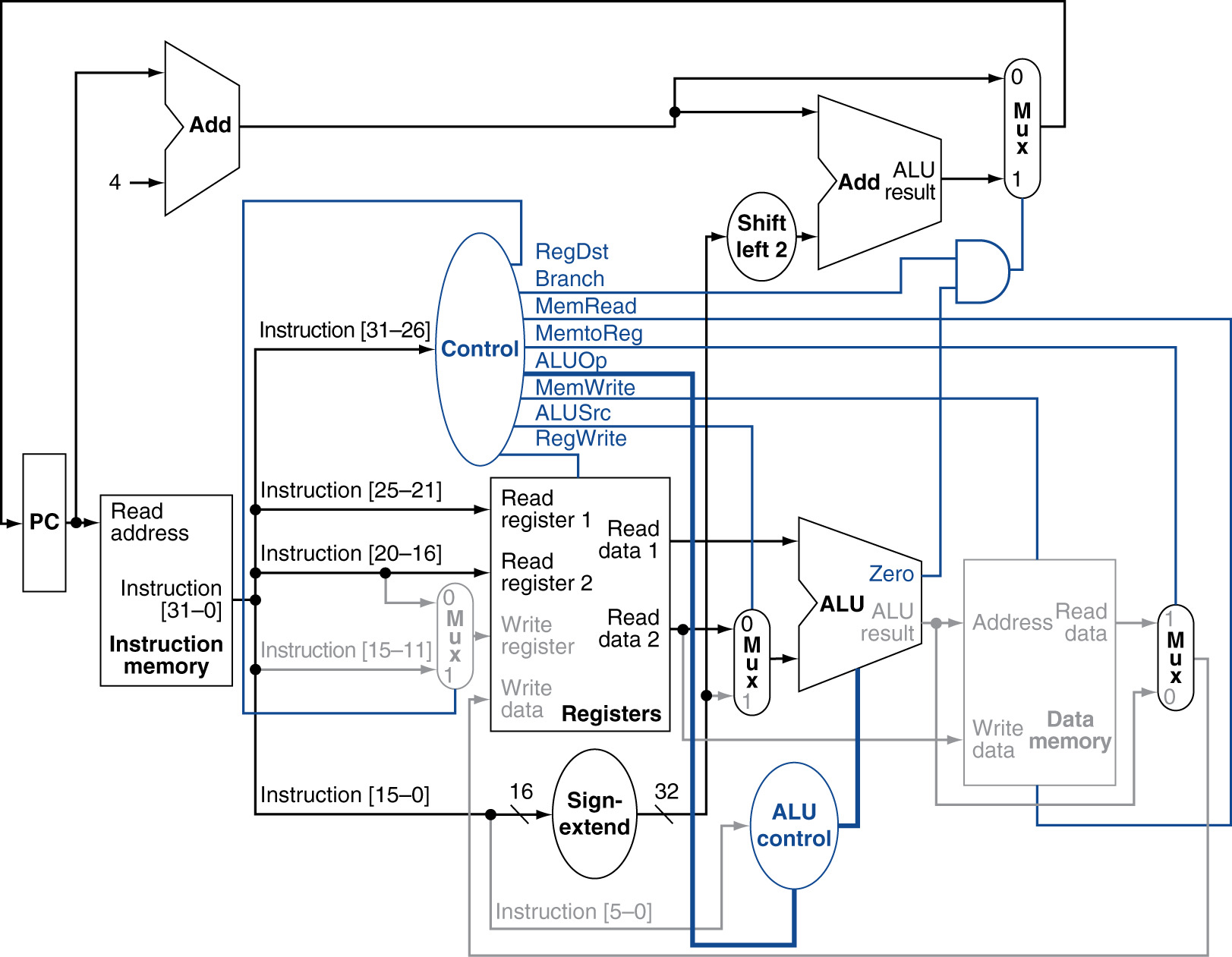
11.6.2 Datapath Elements Used
Load Word Instruction Datapath
Active Elements:
- Instruction Memory: Fetch instruction
- Program Counter & PC+4 Adder
- Register File: Read RS (base); Write RT (destination)
- Sign Extender: Extend offset to 32 bits
- Multiplexer (ALUSrc): Select immediate
- ALU: Add base + offset
- Data Memory: Read at calculated address
- Multiplexer (MemtoReg): Select memory data
- Multiplexer (RegDst): Select RT for write
Inactive Elements:
- Second register read (RT as source): Not used
- Branch circuitry: Not used
11.6.3 Control Signal Values for LW
Exercise Example: LW $8, 32($9)
| Signal | Value | Reason |
|---|---|---|
| RegDst | 0 | Write to RT (bits 16-20), not RD |
| Branch | 0 | Not a branch instruction |
| MemRead | 1 | Reading from data memory |
| MemtoReg | 1 | Write memory data (not ALU result) |
| ALUOp | 00 | Perform ADD for address calculation |
| MemWrite | 0 | Not writing to memory (reading only) |
| ALUSrc | 1 | Add immediate offset (not register) |
| RegWrite | 1 | Write loaded data to destination register |
Detailed Explanations:
RegDst = 0:
- I-type format: Destination in RT field
- Multiplexer selects bits 16-20
- RT = 01000 (register 8)
- Different from R-type (RD field)
Branch = 0:
- Sequential execution
- PC updated to PC + 4
MemRead = 1:
- Enable data memory read
- Essential for memory timing
- Memory outputs data at calculated address
- If 0: Memory output undefined (ignored anyway)
MemtoReg = 1:
- Multiplexer selects memory data
- Input 1: Data memory read output
- Input 0: ALU result (address, not data!)
- Must select memory data for load
ALUOp = 00:
- Address calculation requires ADD
- Base address + offset
- ALU Control = 0010 (ADD)
MemWrite = 0:
- Reading, not writing
- Critical: Prevents memory corruption
- If 1: Would write garbage to memory
ALUSrc = 1:
- Need immediate offset for address calculation
- Multiplexer selects sign-extended immediate
- Input 1: Sign-extended offset
- Input 0: RT value (not used for address calc)
RegWrite = 1:
- Must write loaded data to RT
- Data from memory → Register $8
- If 0: Data lost, load ineffective
11.6.4 Critical Path for Load Word
Longest Delay in Single-Cycle:
- Instruction Memory read
- Register File read (base address)
- Sign Extension
- ALU address calculation
- Data Memory read
- Register write setup
Load Word is the slowest instruction!
- Determines minimum clock period
- All other instructions must wait for this worst case
- Major performance bottleneck
11.7 Store Word Instruction Detailed Analysis
11.7.1 Instruction Format
Encoding Structure (32 bits):
- Bits 26-31: Opcode = 101011 (43) - SW
- Bits 21-25: RS (5 bits) - Base address register
- Bits 16-20: RT (5 bits) - Source data register
- Bits 0-15: Immediate (16 bits) - Address offset
Example: SW $8, 32($9)
Encoding: 101011 01001 01000 0000000000100000
         |Opcode|  RS  |  RT  |    Immediate    |
         |  43  |   9  |   8  |       32        |
Operation: Memory[$9 + 32] = $8
Note: Fixed error in lecture (was "$32", should be "32")
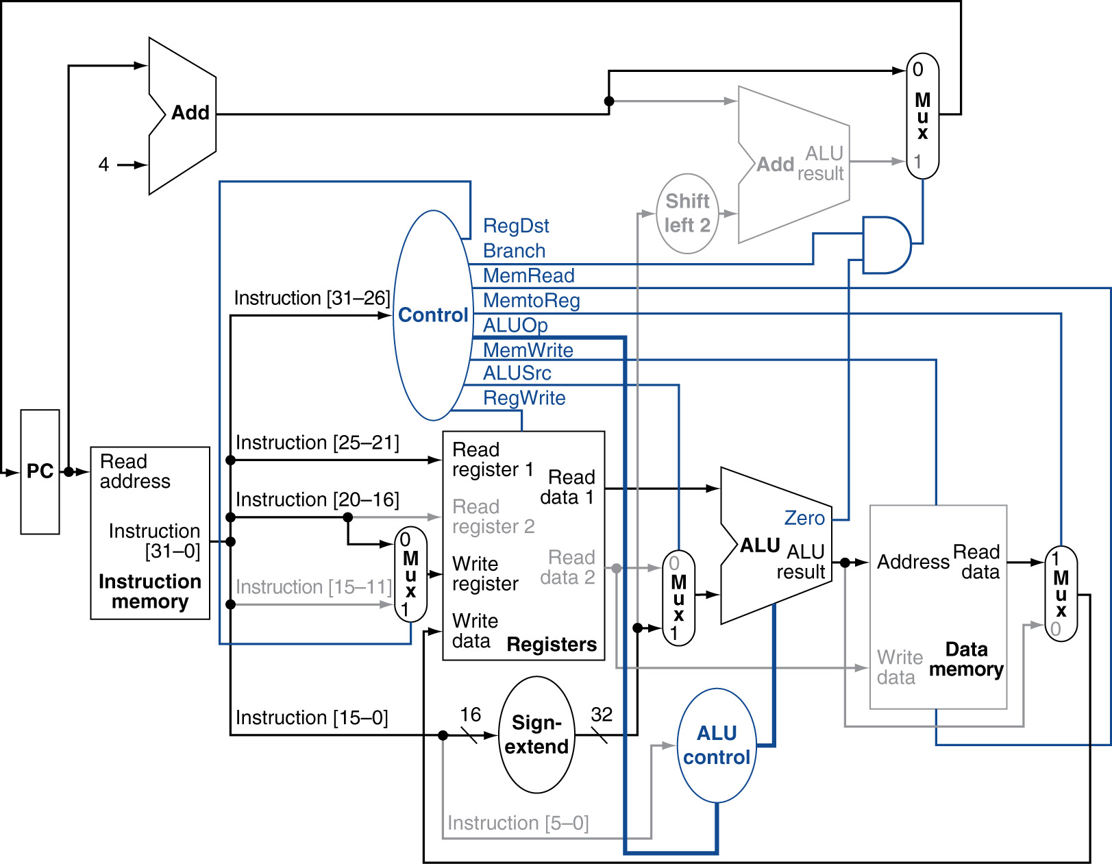
11.7.2 Datapath Elements Used
Active Elements:
- Instruction Memory
- Program Counter & PC+4 Adder
- Register File: Read RS (base) AND RT (data source)
- Sign Extender
- Multiplexer (ALUSrc): Select immediate
- ALU: Add base + offset
- Data Memory: Write RT data at calculated address
Inactive Elements:
- Register Write: No register write
- Memory Read: Writing, not reading
- MemtoReg multiplexer: Output not used
Key Difference from Load:
- TWO register reads: RS for base, RT for data
- Memory write instead of read
- NO register write operation
11.7.3 Control Signal Values for SW
Exercise Example: SW $8, 32($9)
| Signal | Value | Reason |
|---|---|---|
| RegDst | X | Don't care (not writing to register) |
| Branch | 0 | Not a branch instruction |
| MemRead | 0 | Not reading from memory (writing) |
| MemtoReg | X | Don't care (not writing to register) |
| ALUOp | 00 | Perform ADD for address calculation |
| MemWrite | 1 | Writing to data memory |
| ALUSrc | 1 | Add immediate offset |
| RegWrite | 0 | Not writing to register file |
Detailed Explanations:
RegDst = X (Don't Care):
- RegWrite = 0: No register write
- Write address irrelevant
- Could be 0 or 1, doesn't matter
- Using X simplifies logic design
CRITICAL: RegWrite = 0:
- Must prevent register file write
- If RegWrite = 1: Disaster!
- Some register address fed to write port
- Either ALU result (address) or memory data (garbage, MemRead=0)
- Would corrupt random register
- Data integrity violated
Why It Matters:
- Hardware operates in parallel
- Multiplexers produce outputs even if not used
- Without RegWrite = 0:
- RegDst mux outputs some address
- MemtoReg mux outputs some data
- If RegWrite = 1: This garbage written to register!
- Control signal correctness essential
MemRead = 0, MemWrite = 1:
- Writing to memory, not reading
- MemRead = 0: Memory read output undefined
- MemWrite = 1: Memory accepts write data
- Opposite of Load Word
MemtoReg = X (Don't Care):
- RegWrite = 0: Write data source irrelevant
- Output not used
- Even if wrong data selected, RegWrite prevents write
ALUOp = 00:
- Same as Load Word
- Address calculation: ADD operation
ALUSrc = 1:
- Need immediate offset
- Same as Load Word
11.7.4 Important Lesson: Don't Care vs Zero
Student Confusion:
"RegDst = 0 is not wrong, but best answer is X"Clarification:
- Functionally: 0 works (doesn't cause error)
- Logically: X is correct (truly doesn't matter)
- Design perspective: X simplifies Boolean expressions
- Karnaugh map minimization: X allows more groupings
However:
- RegWrite MUST be 0 (not X!)
- MemWrite MUST be correct (not X!)
- Read/Write enables are critical for data integrity
11.8 Jump Instruction Integration
11.8.1 Instruction Format
Encoding Structure (32 bits):
- Bits 26-31: Opcode = 000010 (2) - J
- Bits 0-25: Address (26 bits) - Jump target (word address)
Alternative: JAL (Jump and Link)
- Opcode = 000011 (3)
- Used for function calls
- Saves return address in register $31
Example: J 100
Encoding: 000010 00000000000000000001100100
         |Opcode|     Target Address       |
         |   2  |          100             |
Operation: PC = {PC+4[31:28], Address, 2'b00}
11.8.2 Jump Target Address Calculation
Word Address to Byte Address:
- Target field: 26 bits (word address)
- Shift left by 2: Append 2 zero bits
- Result: 28-bit byte address
Upper 4 Bits:
- Take from PC+4 current value
- Bits 31:28 of next sequential instruction
- Preserves region (256 MB regions)
- Jump within same region as current PC
Concatenation:
PC+4:        [31:28]  [27:2]  [1:0]
                ↓                (ignored)
Jump Target: [31:28] [Target×4] [00]
                ↑         ↑        ↑
              From     From    Append
              PC+4  instruction zeros
Example:
- PC = 0x10000000
- PC+4 = 0x10000004
- Target = 100 = 0x000064
- Shift left 2: 0x000190
- Upper 4 bits: 0x1
- Jump Address: 0x10000190
Limitation:
- Can only jump within 28-bit range (256 MB)
- Upper 4 bits fixed by current PC region
- For larger jumps: Use jump register (JR) instruction
11.8.3 Additional Datapath Hardware

Jump Instruction Datapath with Additional Hardware
New Components:
Shift Left 2 (for jump):
- Input: 26-bit target field
- Output: 28-bit byte offset
- Implementation: Wire routing (no actual shifter!)
Concatenation Logic:
- Input 1: PC+4 bits [31:28] (4 bits)
- Input 2: Shifted target (28 bits)
- Output: 32-bit jump address
- Implementation: Wire concatenation
New Multiplexer:
- Input 0: Output from branch/sequential mux
- Could be PC+4 or branch target
- Input 1: Jump target address (32 bits)
- Select: Jump control signal
- Output: Next PC value
Original PC Source Mux:
- Input 0: PC + 4
- Input 1: Branch target
- Select: PCSrc (Branch AND Zero)
New Jump Mux (outer):
- Input 0: Original mux output (PC+4 or branch target)
- Input 1: Jump target
- Select: Jump signal
- Output: Final next PC value
11.8.4 Jump Control Signal
Jump Signal:
- 10th control output bit
- Generated by Control Unit
- Based on opcode = 2 (J) or 3 (JAL)
Values:
- Jump = 1: Select jump target
- Jump = 0: Select sequential/branch
Other Control Signals for Jump:
| Signal | Value | Reason |
|---|---|---|
| RegDst | X | Don't care |
| Branch | 0 | Not a branch (different mechanism) |
| MemRead | 0 | Not accessing memory |
| MemtoReg | X | Don't care |
| ALUOp | XX | Don't care (ALU not used) |
| MemWrite | 0 | Not writing memory |
| ALUSrc | X | Don't care |
| RegWrite | 0 | Not writing register (J instruction) |
| Jump | 1 | This IS a jump instruction |
Note: JAL (Jump and Link) different:
- RegWrite = 1 (saves return address)
- RegDst = ? (special: write to $31)
- Additional logic needed for return address
11.8.5 Complete Datapath with Jump
All Instruction Types Supported:
- R-type: Arithmetic, logic, shift
- I-type: Load, Store, Branch, Immediate arithmetic
- J-type: Jump, Jump and Link
Coverage:
- 95%+ of MIPS ISA hardware
- Complete single-cycle implementation
- Additional variants (BNE, shifts, etc.) need minor additions
Datapath Completeness:
- Two memories: Instruction and Data
- One ALU for computation
- Multiple adders: PC+4, Branch target
- Many multiplexers for data routing
- Sign extender
- Shift left 2 circuits (wire routing)
- Control unit with 10 control signal bits
11.9 Timing Analysis with Concrete Delays
11.9.1 Assumed Component Delays
Delay Values (in nanoseconds):
| Component | Delay | Notes |
|---|---|---|
| Instruction Memory | 2 ns | Read instruction at PC address |
| Register File (Read) | 1 ns | Output data after address change |
| Register File (Write) | 1 ns | At clock edge (next cycle) |
| Sign Extender | ~0 ns | Negligible (wire replication) |
| Multiplexers | ~0 ns | Negligible compared to other delays |
| ALU Operation | 2 ns | Arithmetic/logic/comparison |
| Data Memory (Read) | 2 ns | Output data after address provided |
| Data Memory (Write) | 2 ns | At clock edge (next cycle) |
| PC+4 Adder | 2 ns | Simple addition |
| Branch Target Adder | 2 ns | Addition with offset |
Assumptions:
- Simplified for analysis
- Real delays depend on technology, circuit design
- Memory accesses typically slowest
- Combinational logic relatively fast
11.9.2 Critical Path Analysis
Definition:
- Longest delay path from clock edge to clock edge
- Determines minimum clock period
- All combinational logic between sequential elements
Single-Cycle Constraint:
- Entire instruction must complete in one clock cycle
- Clock period ≥ Critical path delay
- All instructions take same time (worst case)
11.9.3 Load Word Instruction Timing
Step-by-Step Delay Calculation:
Step 1: Instruction Fetch (2 ns)
- Clock edge: PC updated
- PC → Instruction Memory
- Instruction Memory reads and outputs instruction
- Delay: 2 ns
- Running total: 2 ns
Step 2: Register Read (1 ns)
- Instruction decoded
- RS field extracted
- RS → Register File Read Address 1
- Register File outputs base address
- Delay: 1 ns
- Running total: 2 + 1 = 3 ns
Step 3: Sign Extension (~0 ns)
- Immediate field extracted
- Sign extended to 32 bits
- Delay: Negligible
- Running total: ~3 ns
Step 4: ALU Address Calculation (2 ns)
- Base address + offset
- ALU performs addition
- Output: Memory address
- Delay: 2 ns
- Running total: 3 + 2 = 5 ns
Step 5: Memory Read (2 ns)
- ALU result → Data Memory address
- MemRead = 1 asserted
- Data Memory reads and outputs data
- Delay: 2 ns
- Running total: 5 + 2 = 7 ns
Step 6: Register Write Setup (~0 ns)
- Memory data → Register Write Data input
- RT → Register Write Address
- Ready for clock edge
- Delay: Setup time negligible
- Running total: ~7 ns
Clock Edge: Register Write (next cycle)
- At next positive clock edge
- Data written to register
- Takes 1 ns but in next cycle
Minimum Clock Period: 7 nanoseconds
Maximum Clock Frequency: 1/7 ns ≈ 143 MHz
Load Word is Critical Path!
- Longest instruction in single-cycle design
- Determines clock period for ALL instructions
11.9.4 Store Word Instruction Timing
Step-by-Step Delay:
- Instruction Fetch: 2 ns (total: 2 ns)
- Register Read: 1 ns (total: 3 ns)
- Read RS (base) AND RT (data)
- Sign Extension: ~0 ns (total: 3 ns)
- ALU Address Calculation: 2 ns (total: 5 ns)
- Memory Write Setup: ~0 ns (total: 5 ns)
- Address and data ready at memory inputs
Clock Edge: Memory Write (end of cycle)
- Data written to memory at clock edge
- Takes 2 ns but next instruction fetch also 2 ns
- Next instruction register read starts after 3 ns total
- Memory write completes before register read needs data
- No conflict
Minimum Time Required: 5 nanoseconds
Note:
- Faster than Load Word (no memory read delay)
- But must use 7 ns clock period anyway (single-cycle)
- Wastes 2 ns per Store instruction
11.9.5 Arithmetic Instruction Timing (ADD, SUB, AND, OR)
Step-by-Step Delay:
- Instruction Fetch: 2 ns (total: 2 ns)
- Register Read: 1 ns (total: 3 ns)
- Read RS and RT
- ALU Operation: 2 ns (total: 5 ns)
- Perform arithmetic/logic operation
- Register Write Setup: ~0 ns (total: 5 ns)
- ALU result ready at register write data input
Clock Edge: Register Write
- Result written to RD
Minimum Time Required: 5 nanoseconds
Efficiency Loss:
- Could run at 5 ns clock period
- Forced to wait 7 ns (Load Word limitation)
- Wastes 2 ns = 28.6% time wasted per R-type instruction
11.9.6 Branch Instruction Timing
Step-by-Step Delay:
- Instruction Fetch: 2 ns (total: 2 ns)
- Register Read: 1 ns (total: 3 ns)
- Read RS and RT for comparison
- ALU Comparison: 2 ns (total: 5 ns)
- Subtract RS - RT
- Generate Zero flag
- Branch Target Calculation: 2 ns (parallel with ALU)
- Sign extend offset: ~0 ns
- Shift left 2: ~0 ns (wire routing)
- Add to PC+4: 2 ns
- Can happen in parallel with ALU operation!
- PC Update Setup: ~0 ns (total: 5 ns)
- Zero flag + Branch → PCSrc
- Multiplexer selects next PC
- Ready for clock edge
Minimum Time Required: 5 nanoseconds
Key Insight:
- Branch target calculation parallel to ALU
- PC+4 already available from fetch stage
- No memory access needed
- Fast like R-type
11.9.7 Jump Instruction Timing
Step-by-Step Delay:
- Instruction Fetch: 2 ns (total: 2 ns)
- Also calculates PC+4 in parallel
- Jump Target Calculation: ~0 ns
- Extract 26-bit target
- Shift left 2: Wire routing, ~0 ns
- Concatenate with PC+4[31:28]: Wire connection, ~0 ns
- No ALU, no memory, no registers!
- PC Update Setup: ~0 ns (total: 2 ns)
Minimum Time Required: 2 nanoseconds
Fastest Instruction:
- Only instruction fetch needed
- Jump target calculation: Wire operations only
- No sequential dependencies
- Wastes 5 ns waiting for clock period!
11.9.8 Timing Summary Table
| Instruction Type | Time Required | Wasted Time | Efficiency |
|---|---|---|---|
| Load Word (LW) | 7 ns | 0 ns | 100% |
| Store Word (SW) | 5 ns | 2 ns | 71.4% |
| R-type (ADD, etc.) | 5 ns | 2 ns | 71.4% |
| Branch (BEQ) | 5 ns | 2 ns | 71.4% |
| Jump (J) | 2 ns | 5 ns | 28.6% |
Clock Period (Single-Cycle): 7 ns (determined by LW)
Clock Frequency: ~143 MHz
Performance Impact:
- Most instructions waste time
- Only Load Word fully utilizes clock cycle
- Tremendous inefficiency
11.10 Performance Analysis
11.10.1 Program Composition Example
Typical MIPS Program Profile:
| Instruction Type | Percentage | Time if Variable | Time (Fixed 7ns) |
|---|---|---|---|
| Arithmetic | 48% | 5 ns | 7 ns |
| Load Word | 22% | 7 ns | 7 ns |
| Store Word | 11% | 5 ns | 7 ns |
| Branch | 19% | 5 ns | 7 ns |
11.10.2 Average Time Calculation
Variable Time (Ideal):
Average = (0.48 × 5) + (0.22 × 7) + (0.11 × 5) + (0.19 × 5)
        = 2.40 + 1.54 + 0.55 + 0.95
        = 5.44 ns per instruction
Single-Cycle (Actual):
Average = 7 ns per instruction (all instructions)
Performance Loss:
Overhead = 7 - 5.44 = 1.56 ns per instruction
Efficiency = 5.44 / 7 = 77.7%
Waste = 22.3% of time
11.10.3 Critical Path Problem
Critical Path Determination:
- Load Word uses most datapath elements
- Sequential dependencies:
- Instruction Memory
- Register File
- ALU
- Data Memory
- (Register Write in next cycle)
Design Principle Violation:
- "Make the common case fast"
- Common case: Arithmetic instructions (48%)
- Slow case (Load Word) determines speed
- Common case forced to slow down
- Design is inefficient
11.10.4 Clock Period Inflexibility
Single-Cycle Constraint:
- Clock period MUST be constant
- Cannot vary by instruction
- Must accommodate worst case (slowest instruction)
- All faster instructions penalized
Implications:
- Arithmetic: Could run at 143 MHz, forced to 143 MHz ✓
- Load: Needs 143 MHz, gets 143 MHz ✓
- Jump: Could run at 500 MHz, forced to 143 MHz ✗
Efficiency by Instruction:
| Instruction | Efficiency | Waste |
|---|---|---|
| Jump | 28.6% | 71.4% |
| Arithmetic | 71.4% | 28.6% |
| Store | 71.4% | 28.6% |
| Branch | 71.4% | 28.6% |
| Load | 100.0% | 0% |
11.11 Path to Better Performance: Multi-Cycle Design
11.11.1 Multi-Cycle Concept
Basic Idea:
- Break instruction execution into multiple stages
- Each stage completes in one (shorter) clock cycle
- Different instructions use different number of cycles
- Only use stages actually needed
Advantages:
- Shorter clock period (faster clock)
- Instructions take only time they need
- Better average performance
- More efficient resource utilization
11.11.2 Stage Division
Typical Stages:
Stage 1: Instruction Fetch (IF)
- Read from instruction memory
- Update PC to PC+4
- Store instruction in register
Stage 2: Instruction Decode (ID)
- Decode opcode
- Read registers
- Generate control signals
- Sign extend immediate
Stage 3: Execute (EX)
- ALU operation
- Or address calculation
- Or branch comparison
Stage 4: Memory Access (MEM)
- Read from data memory (if load)
- Write to data memory (if store)
- Or skip this stage
Stage 5: Write-Back (WB)
- Write result to register file
- Or skip if no write needed
Not All Instructions Use All Stages:
- R-type: IF, ID, EX, WB (skip MEM) = 4 cycles
- Load: IF, ID, EX, MEM, WB (all stages) = 5 cycles
- Store: IF, ID, EX, MEM (skip WB) = 4 cycles
- Branch: IF, ID, EX (skip MEM, WB) = 3 cycles
- Jump: IF, ID (skip EX, MEM, WB) = 2 cycles
11.11.3 Clock Period in Multi-Cycle
Determining Clock Period:
- Clock period = Longest stage delay
- NOT longest instruction delay
- Much shorter than single-cycle
Example Stage Delays:
| Stage | Delay |
|---|---|
| IF (Instr Memory) | 2 ns |
| ID (Register Read) | 1 ns |
| EX (ALU) | 2 ns |
| MEM (Data Memory) | 2 ns |
| WB (Register Write) | 1 ns |
Longest Stage: 2 ns
Clock Period: 2 ns (vs 7 ns single-cycle)
Clock Frequency: 500 MHz (vs 143 MHz single-cycle)
11.11.4 Performance Comparison
Single-Cycle:
All instructions: 1 cycle × 7 ns = 7 ns
Multi-Cycle (with 2 ns clock):
| Instruction | Cycles | Time |
|---|---|---|
| Arithmetic | 4 | 8 ns |
| Load | 5 | 10 ns |
| Store | 4 | 8 ns |
| Branch | 3 | 6 ns |
| Jump | 2 | 4 ns |
Weighted Average (same program profile):
Average = (0.48 × 8) + (0.22 × 10) + (0.11 × 8) + (0.19 × 6)
        = 3.84 + 2.20 + 0.88 + 1.14
        = 8.06 ns per instruction
Wait, That's Worse!
- Multi-cycle: 8.06 ns average
- Single-cycle: 7 ns always
- Multi-cycle slower?!
Resolution:
- Example delays assumed equal stage times
- In reality, stages have different delays
- Need to balance stage delays
- Goal: Make all stages approximately equal
- Then multi-cycle becomes efficient
Ideal Multi-Cycle (balanced 1.4 ns stages):
| Instruction | Cycles | Time |
|---|---|---|
| Arithmetic | 4 | 5.6 ns |
| Load | 5 | 7.0 ns |
| Store | 4 | 5.6 ns |
| Branch | 3 | 4.2 ns |
Average = (0.48 × 5.6) + (0.22 × 7.0) + (0.11 × 5.6) + (0.19 × 4.2)
        = 2.69 + 1.54 + 0.62 + 0.80
        = 5.65 ns per instruction

Speedup = 7 / 5.65 = 1.24× faster
11.11.5 Design Challenge
Stage Balancing:
- Goal: Roughly equal delay per stage
- Challenge: Memory slower than ALU
- Memory stage limits clock period
- Need techniques:
- Faster memory
- Cache memory (next topic)
- Pipeline (next lecture)
Resource Reuse:
- Single ALU used across multiple cycles
- Single memory port can be reused
- Fewer hardware resources needed
- More control complexity (FSM needed)
11.12 Preview: Pipelining
11.12.1 Next Step Beyond Multi-Cycle
Pipelining Concept:
- Multiple instructions in flight simultaneously
- Each instruction at different stage
- Like assembly line
- Stage 1: Fetch instruction A
- Stage 2: Decode A, Fetch B
- Stage 3: Execute A, Decode B, Fetch C
- Stage 4: Memory A, Execute B, Decode C, Fetch D
- Stage 5: Write A, Memory B, Execute C, Decode D, Fetch E
Benefits:
- One instruction completes per cycle (like single-cycle)
- But clock period short (like multi-cycle)
- Best of both worlds
- Dramatic performance improvement
Challenges (Covered Next Lecture):
- Hazards: Data dependencies between instructions
- Control hazards: Branches affect pipeline
- Structural hazards: Resource conflicts
- Need forwarding and stall logic
- More complex control
11.12.2 Coming Next
Topics:
- Pipelined datapath design
- Hazard detection and resolution
- Forwarding (bypassing)
- Branch prediction
- Performance analysis
- MIPS pipeline implementation
Key Takeaways
- Single-cycle design executes each instruction in one clock cycle, with clock period determined by the slowest instruction (Load Word at 7 ns).
- Control unit generates signals based on opcode, orchestrating datapath operations for R-type, Load, Store, Branch, and Jump instructions.
- Load Word is the critical path (Instruction Fetch → Register Read → ALU → Memory Read → Register Write), determining minimum clock period.
- Jump instruction uses PC[31:28] concatenated with shifted immediate to form 32-bit target address, enabling 256 MB jump range.
- Control signals must prevent data corruption, with RegWrite=0 for Store and Branch to avoid unintended register modifications.
- "Don't care" values (X) simplify control logic, allowing optimization when signals don't affect instruction outcome.
- Hardware operates concurrently, not sequentially—multiple operations happen simultaneously within each clock cycle.
- Performance inefficiency drives design evolution, as most instructions finish early but must wait for full clock period.
- Resource utilization varies dramatically, with arithmetic instructions using ~43% of clock period while Load uses 100%.
- Timing analysis reveals optimization opportunities, showing that memory access dominates critical path (4 ns of 7 ns total).
- Write operations occur at clock edge, ensuring data stability and preventing race conditions in sequential logic.
- Branch target calculation happens in parallel with ALU comparison, optimizing branch instruction timing.
- Sign extension is effectively instantaneous (combinational logic), adding negligible delay to critical path.
- Clock period sets maximum frequency (~143 MHz for 7 ns period), directly impacting overall processor performance.
- Common case (arithmetic) runs slowly, violating fundamental design principle of making common case fast.
- Stage division concept emerges from timing analysis, suggesting multi-cycle implementation could improve efficiency.
- Control signal truth tables systematically define behavior, mapping each instruction to specific control patterns.
- PC update mechanisms vary by instruction type, using PC+4, branch target, or jump target based on control signals.
- Data memory access only for Load/Store, with MemRead and MemWrite controlling when memory participates in execution.
- Performance analysis quantifies inefficiency, providing concrete motivation for pipelined processor designs in subsequent lectures.
Summary
The single-cycle MIPS processor represents a complete, functioning implementation where each instruction executes in exactly one clock cycle. While conceptually straightforward and easy to understand, the design reveals fundamental performance limitations that drive modern processor architecture evolution. The critical path analysis shows Load Word requiring 7 nanoseconds while simpler instructions like arithmetic operations complete in just 3 nanoseconds, forcing all instructions to wait for the slowest operation. This inefficiency—with most instructions utilizing less than half the available clock period—violates the crucial design principle of "making the common case fast." The systematic control signal analysis demonstrates how the control unit orchestrates datapath operations for different instruction types (R-type, Load, Store, Branch, Jump), with careful attention to preventing data corruption through proper RegWrite and MemWrite signals. The jump instruction introduces pseudo-direct addressing, concatenating PC upper bits with shifted immediate for 256 MB addressability. While the single-cycle design provides essential conceptual foundation for understanding processor operation, the detailed timing analysis and resource utilization metrics clearly motivate the need for more sophisticated approaches—multi-cycle processors that divide execution into variable-length stages, and pipelined processors that overlap instruction execution for dramatically improved throughput. These performance limitations aren't flaws but rather inevitable consequences of the single-cycle constraint, establishing why modern processors universally adopt pipelining despite the additional complexity it introduces.