Click the thumbnail above to watch the video lecture on YouTube
13.1 Introduction
This lecture provides comprehensive, cycle-by-cycle analysis of MIPS five-stage pipeline operation, examining how instructions flow through pipeline stages with detailed attention to the pipeline registers that store intermediate results between stages. We explore the critical role of these registers in enabling independent stage operation, trace complete execution sequences for load and store instructions, analyze timing constraints and delay contributions, and work through practical exercises calculating clock frequencies and optimizing pipeline performance. This detailed examination reveals the hardware mechanisms that transform the conceptual pipeline model into functioning silicon.
13.2 Lecture Introduction and Recap
13.2.1 Previous Topics Review
Pipelining Concept:
- Instruction-level parallelism exploitation
- Five-stage MIPS pipeline: IF, ID, EX, MEM, WB
- Staggered instruction execution
- All hardware utilized simultaneously
Performance Metric:
- Throughput improved (not latency)
- Instructions/unit time increased
- Individual instruction latency same or worse
- Overall system performance dramatically better
Hazards Covered:
- Structural: Hardware resource conflicts
- Data: Register/memory dependencies
- Control: Branch/jump decision delays
Solutions Discussed:
- Structural: Separate I-cache and D-cache
- Data: Forwarding, code reordering
- Control: Early branch resolution, prediction
13.2.2 Today's Focus
Detailed Pipeline Analysis:
- Cycle-by-cycle operation walkthrough
- Pipeline register requirements
- Timing and delay analysis
- Load/Store instruction examples
- Common implementation errors
- Practical exercises
13.3 Five-Stage MIPS Pipeline Review
Five-Stage MIPS Pipeline Architecture
13.3.1 Stage 1: Instruction Fetch (IF)
Operations:
- PC value determines instruction address
- Access instruction memory
- Fetch 32-bit instruction word
- Calculate PC + 4 for next sequential instruction
Hardware Elements:
- Program Counter register
- Instruction Memory
- PC + 4 Adder
Key Point:
- Both operations (memory read, PC+4 calculation) occur in parallel
13.3.2 Stage 2: Instruction Decode / Register Read (ID)
Operations:
- Decode opcode (6 bits)
- Determine instruction type
- Identify register fields
- Read register file (RS, RT)
- Sign-extend immediate value (16→32 bits)
- Generate control signals
Hardware Elements:
- Instruction decoder (combinational logic)
- Register file (read ports)
- Sign extension unit
- Control unit
Workload Balancing:
- Decode + register read fit in one cycle
- Even distribution of work
- Register read dominates timing
Control Signal Generation:
- 9-10 control signal bits generated
- Based on opcode
- Used by subsequent stages
- Must be preserved through pipeline
13.3.3 Stage 3: Execution (EX)
Operations:
- ALU performs computation OR address calculation
- Multiplexer selects second operand (register vs immediate)
- Branch: Compare registers, compute target address
Hardware Elements:
- ALU (Arithmetic Logic Unit)
- Input multiplexer (register/immediate selection)
- Branch target adder (parallel to ALU)
- Shift left 2 unit (for branch offset)
Key Characteristics:
- ALU operation dominates timing
- Branch hardware operates in parallel
- Multiple functions depending on instruction type
13.3.4 Stage 4: Memory Access (MEM)
Operations:
- Load: Read from data memory
- Store: Write to data memory
- Other instructions: Skip (no memory access)
- Branch: PC update decision
Hardware Elements:
- Data Memory
- PC source multiplexer (for branches)
Timing Consideration:
- Memory access slowest operation
- Dominates stage timing
- Critical path component
13.3.5 Stage 5: Write Back (WB)
Operations:
- Select data source (ALU result OR memory data)
- Write to destination register
- Load: Memory data → register
- Arithmetic: ALU result → register
Hardware Elements:
- MemtoReg multiplexer
- Register file (write port)
Minimal Hardware:
- Mostly multiplexer visible
- Register file shared with ID stage
- Shortest stage conceptually
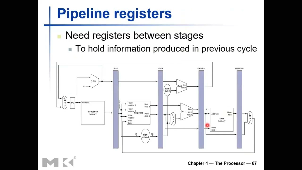
13.4 Pipeline Registers: Necessity and Function
13.4.1 Problem Without Pipeline Registers
Scenario:
- Multiple instructions in different stages
- All sharing same hardware components
- Data from different instructions
Example Issues:
- Register file: ID stage reads while WB stage writes
- Control signals: Generated in ID, needed in later stages
- Data values: Computed in EX, needed in MEM
- Overwriting: New instruction data overwrites previous instruction data
Result Without Pipeline Registers:
- Data hazards everywhere
- Control hazards from signal conflicts
- Structural hazards from resource contention
- Pipeline cannot function correctly
13.4.2 Pipeline Register Purpose
Pipeline Registers Between Pipeline Stages
Key Function:
- Store information from previous stage
- Make data available to next stage
- Synchronize operations across clock cycles
- Prevent interference between instructions
Placement:
- One between each pair of consecutive stages
- IF/ID: Between instruction fetch and decode
- ID/EX: Between decode and execution
- EX/MEM: Between execution and memory
- MEM/WB: Between memory and write back
Exception:
- No register between WB and IF
- PC register serves this purpose
- Register file contains storage
- No additional register needed
13.4.3 Pipeline Register Contents
IF/ID Pipeline Register:
- 32-bit instruction word
- 32-bit PC+4 value
- Total: 64 bits
ID/EX Pipeline Register:
- Two 32-bit register values (from register file)
- 32-bit sign-extended immediate
- 32-bit PC+4 value (for branches)
- 5-bit write register address
- 9-10 control signal bits
- Total: ~140+ bits (largest pipeline register)
EX/MEM Pipeline Register:
- 32-bit ALU result
- 32-bit register value (for stores)
- 32-bit branch target address
- 1-bit ALU zero flag
- 5-bit write register address
- Control signals for MEM/WB stages
- Total: ~105+ bits
MEM/WB Pipeline Register:
- 32-bit memory read data
- 32-bit ALU result
- 5-bit write register address
- Control signals for WB stage
- Total: ~75+ bits
13.4.4 Timing: Writing and Reading Pipeline Registers
At Rising Clock Edge:
- Pipeline register write begins
- Small hold time delay (~10-30 ps)
- Data captured and stored
- Writing delay consumed
After Writing:
- Reading delay begins
- Data propagates to output (~10-30 ps)
- Outputs stabilize at new values
- Next stage begins operations
Combined Overhead:
- Write delay + read delay = ~20-60 ps
- Occurs at start of every stage
- Reduces time available for actual computation
- Pipelining overhead cost
Critical Observation:
- These delays don't exist in single-cycle
- Pipelining adds latency overhead
- But throughput gain outweighs latency cost
13.5 Load Word Instruction: Detailed Cycle-by-Cycle Analysis
13.5.1 Load Word Instruction Format
Encoding:
LW $rt, offset($rs)

Opcode: 100011 (bits 26-31)
RS:     Base register (bits 21-25)
RT:     Destination register (bits 16-20)
Offset: 16-bit immediate (bits 0-15)
Operation: $rt = Memory[$rs + offset]
Example: LW $8, 32($9)
- Base address in $9
- Add offset 32
- Load from memory into $8
13.5.2 Clock Cycle 1: Instruction Fetch (IF)
Start of Cycle:
- New PC value available (from previous cycle)
- PC write delay: ~10-30 ps
- PC read delay: ~10-30 ps
Operations:
- Update PC register (rising edge)
- Read PC value (small delay)
- Access instruction memory with PC address
- Instruction memory read delay: ~200 ps (dominant)
- Compute PC + 4 in parallel: ~70 ps
End of Cycle:
- 32-bit LW instruction available
- PC + 4 value available
- Both ready to write to IF/ID register
Hardware Shading Convention:
- Right side shaded: Device READ
- Left side shaded: Device WRITTEN
- Example: Instruction Memory right-side shaded (read)
- IF/ID register left-side shaded (written to)
Total Stage Time: ~200+ ps (instruction memory dominant)
13.5.3 Clock Cycle 2: Instruction Decode / Register Read (ID)
Start of Cycle (Rising Edge):
- IF/ID register write: ~30 ps
- IF/ID register read: ~30 ps
- Combined delay: ~60 ps
After Pipeline Register:
- Instruction word available
- Extract fields:
- Opcode: bits 26-31 → Control Unit
- RS (bits 21-25) → Register file address 1
- RT (bits 16-20) → Register file address 2 AND write address
- Offset (bits 0-15) → Sign extender
Parallel Operations:
- Control Unit: Decode opcode → Generate control signals (~50 ps)
- Register File: Read RS ($9) and RT ($8 address, value not needed)
- Read delay: ~90 ps (dominant)
- Sign Extender: Extend 32 to 32 bits (~10 ps, negligible)
End of Cycle:
- Base address value (from $9) available
- RT address read (discarded for LW)
- Sign-extended offset (32) available
- PC + 4 value forwarded
- Control signals generated
- All ready for ID/EX register
Why Read Both Registers:
- Hardware simplicity: Always read both
- Multiplexer decides usage later
- Store would need RT value
- Simpler than conditional reading
Total Stage Time: ~60 + 90 = ~150 ps (register read dominant)
13.5.4 Clock Cycle 3: Execution (EX)
Start of Cycle:
- ID/EX register write: ~30 ps
- ID/EX register read: ~30 ps
ALU Input Preparation:
- Input A: Base address (from $9) directly from pipeline register
- Input B: Multiplexer selects immediate OR register
- Control signal ALUSrc = 1 (select immediate)
- Multiplexer delay: ~20 ps
- Sign-extended offset (32) selected
ALU Operation:
- Add base address + offset
- ALU delay: ~90 ps (dominant)
- Result: Memory address = $9 + 32
Parallel Operations (for branches, not used here):
- Shift left 2: Offset × 4 (~10 ps)
- Branch target adder: PC+4 + (offset×4) (~70 ps)
- Zero flag generation
End of Cycle:
- Memory address available at ALU output
- Branch target available (unused)
- Zero flag available (unused)
- RT value forwarded (unused for LW)
- Control signals forwarded
- Write register address (RT) forwarded
- All ready for EX/MEM register
Total Stage Time: ~30 + 30 + 20 + 90 = ~170 ps (ALU dominant)
13.5.5 Clock Cycle 4: Memory Access (MEM)
Start of Cycle:
- EX/MEM register write: ~30 ps
- EX/MEM register read: ~30 ps
Memory Access:
- ALU result (address) → Data memory address input
- MemRead control signal = 1 (enable read)
- MemWrite control signal = 0 (disable write)
- Data memory read delay: ~250 ps (DOMINANT - slowest operation!)
Parallel Operations (unused for LW):
- Zero flag + Branch → PCSrc decision
- Branch target → PC multiplexer
End of Cycle:
- Loaded data available from memory
- ALU result (address) forwarded for R-type instructions
- Write register address (RT) forwarded
- Control signals forwarded
- All ready for MEM/WB register
Critical Path:
- Load Word determines minimum clock period
- Memory access slowest component
- All other instructions wait for this
Total Stage Time: ~30 + 30 + 250 = ~310 ps (memory READ dominant!)
13.5.6 Clock Cycle 5: Write Back (WB)
Start of Cycle:
- MEM/WB register write: ~30 ps
- MEM/WB register read: ~30 ps
Data Selection:
- MemtoReg multiplexer:
- Control signal MemtoReg = 1 (select memory data)
- Input 0: ALU result (not used for LW)
- Input 1: Memory read data (SELECTED)
- Multiplexer delay: ~20 ps
Register Write Preparation:
- Write data: Memory data from multiplexer
- Write address: RT ($8) from pipeline register
- RegWrite control signal = 1 (enable write)
CRITICAL ERROR IN TEXTBOOK DIAGRAM:
- Many diagrams show write address from IF/ID register
- WRONG! IF/ID has current instruction (4 cycles later!)
- Correct: Write address propagated through ALL pipeline registers
- Must use write address from MEM/WB register
At Rising Edge (End of Cycle / Start of Next):
- Register $8 written with loaded data
- Write occurs in first half of cycle
- Subsequent ID stage can read in second half (same cycle!)
Register File Timing Trick:
- Write: First half of clock cycle
- Read: Second half of clock cycle
- Enables read-after-write in adjacent cycles
- Critical for data forwarding
13.5.7 Load Word Complete Pipeline Summary
| Cycle | Stage | Operations | Dominant Delay | Time |
|---|---|---|---|---|
| 1 | IF | Fetch instruction, PC+4 | Inst Memory | 200ps |
| 2 | ID | Decode, read regs, control | Reg Read | 150ps |
| 3 | EX | ALU: base + offset | ALU | 170ps |
| 4 | MEM | Read data memory | Memory Read | 310ps ← CRITICAL! |
| 5 | WB | Select memory, write register | Multiplexer | 80ps |
Minimum Clock Period: 310 ps (limited by MEM stage)
Maximum Clock Frequency: 1 / 310ps ≈ 3.2 GHz
Pipeline Overhead:
- Pipeline register delays: ~(30+30) × 5 stages = 300ps
- Actual useful work: ~(200+90+90+250) = 630ps
- Total latency: ~930ps
- Overhead: ~32% of execution time
Comparison to Single-Cycle:
- Single-cycle latency: ~800 ps (no pipeline register overhead)
- Pipelined latency: ~930 ps (with overhead)
- But pipelined throughput: 5× better (ideally)
13.6 Store Word Instruction: Key Differences
13.6.1 Store Word Instruction Format
Encoding:
SW $rt, offset($rs)

Opcode: 101011 (bits 26-31)
RS:     Base register (bits 21-25)
RT:     Source data register (bits 16-20)
Offset: 16-bit immediate (bits 0-15)
Operation: Memory[$rs + offset] = $rt
Example: SW $8, 32($9)
- Base address in $9
- Add offset 32
- Store $8 value to memory
Key Difference from Load:
- RT is SOURCE (not destination)
- RT value needed for memory write
Stages IF, ID, EX: Same as Load Word
Instruction Fetch: Identical to LW
Instruction Decode: Identical to LW
- Read both RS and RT
- RT value NOW IMPORTANT (not discarded)
- Sign-extend offset
Execution: Identical to LW
- Compute memory address: base + offset
- ALU operation same
13.6.2 Memory Access Stage: KEY DIFFERENCE
Start of Cycle:
- EX/MEM register contains:
- Memory address (from ALU)
- RT data value (from register file, preserved through pipeline)
Memory Access:
- Address → Data memory address input
- RT value → Data memory write data input
- MemWrite = 1 (ENABLE write)
- MemRead = 0 (DISABLE read)
Operation:
- Write RT value to computed address
- Memory write delay: ~250 ps
End of Cycle:
- Data written to memory
- Memory read output INVALID (MemRead=0)
- Not used by subsequent stage
Control Signal Critical:
| Control Signal | Load | Store |
|---|---|---|
| MemRead | 1 | 0 |
| MemWrite | 0 | 1 |
| RegWrite (WB stage) | 1 | 0 ← CRITICAL! |
13.6.3 Write Back Stage: NO OPERATION
Store Word WB Stage:
- NO register write needed
- Store wrote to MEMORY (not register)
- RegWrite = 0 (DISABLE)
Why RegWrite MUST Be 0:
- Pipeline registers still contain data
- MemtoReg multiplexer produces output
- If RegWrite = 1: DISASTER!
- Random data written to random register
- Data corruption
- Program failure
Hardware Still Operates:
- Multiplexer produces output (garbage)
- Write address present (RT from pipeline)
- Write data present (memory output = invalid, or ALU result)
- But RegWrite = 0 prevents write
Lesson: Control Signals Essential
- Must prevent unwanted operations
- Hardware runs in parallel
- Only control signals prevent corruption
Store Word Pipeline Summary:
| Cycle | Stage | Operations | Notes |
|---|---|---|---|
| 1 | IF | Fetch SW instruction | Same as LW |
| 2 | ID | Decode, read RS, RT | RT value USED (not discarded) |
| 3 | EX | Compute address | Same as LW |
| 4 | MEM | Write RT to memory | WRITE instead of read |
| 5 | WB | Nothing (bubble) | RegWrite=0, stage idle |
13.7 Common Pipeline Diagram Errors
13.7.1 Error 1: Write Register Address Source
Incorrect Diagram Shows:
- Write register address from IF/ID pipeline register
- Connected directly to register file write port
Why This Is Wrong:
- IF/ID contains CURRENT instruction (just fetched)
- Write back for instruction 4 cycles ago
- Wrong register would be written!
Example:
Cycle 1: LW $8, 0($10) fetched  (IF)
Cycle 2: LW $9, 4($10) fetched  (IF), LW $8 in ID
Cycle 3: LW $10, 8($10) fetched (IF), LW $8 in EX
Cycle 4: ADD $11, $12, $13 fetched (IF), LW $8 in MEM
Cycle 5: SUB $14, $15, $16 fetched (IF), LW $8 in WB

At Cycle 5:
• IF/ID contains SUB (writes $14)
• WB should write $8 (from LW)
• If using IF/ID: Would write to $14 instead of $8!
• WRONG REGISTER!
Correct Implementation:
- Propagate write address through ALL pipeline registers
- ID/EX stores it
- EX/MEM stores it
- MEM/WB stores it
- WB uses address from MEM/WB register
Additional Lines Required:
- 5-bit write address bus through each pipeline register
- Increases pipeline register size
- Essential for correctness
13.7.2 Error 2: Incorrect Memory Access Indication
Diagram Error from Textbook:
- ADD instruction shown accessing data memory (wrong!)
- LW instruction shown NOT accessing data memory (wrong!)
Correct Resource Usage:
| Instruction | IF | ID | EX | MEM | WB |
|---|---|---|---|---|---|
| LW | ✓ | ✓ | ✓ | ✓ Read | ✓ Write Reg |
| SW | ✓ | ✓ | ✓ | ✓ Write | No action |
| ADD | ✓ | ✓ | ✓ | ✗ No access | ✓ Write Reg |
| BEQ | ✓ | ✓ | ✓ | ✗ PC update | ✗ No write |
Shading Convention:
- Shaded box: Resource USED
- Unshaded box: Resource NOT USED (idle)
ADD Instruction Correct:
- MEM stage: No memory access, stage mostly idle
- Just forwards ALU result
LW Instruction Correct:
- MEM stage: Read from data memory
- Memory data forwarded to WB
13.7.3 Error 3: Store Word Memory Read
Another Common Error:
- Store instruction shown with MemRead = 1
- Memory output shown as valid
Why Wrong:
- Store WRITES to memory (MemWrite = 1)
- Should NOT read (MemRead = 0)
- Memory read output undefined/invalid
Correct:
- MemWrite = 1, MemRead = 0
- Memory input: Address and write data
- Memory output: Ignored (invalid)
13.8 Multi-Clock-Cycle Pipeline Diagrams
13.8.1 Single-Clock vs Multi-Clock Diagrams
Single-Clock-Cycle Diagram:
- Shows ONE stage at ONE clock cycle
- Detailed resource usage
- Specific delays visible
- Good for understanding individual stage
Multi-Clock-Cycle Diagram:
- Shows MULTIPLE instructions at MULTIPLE cycles
- Cross-sectional view of pipeline
- Parallel execution visible
- Good for understanding overall flow
13.8.2 Traditional Multi-Cycle Diagram
Format:
Cycle:     1    2    3    4    5    6    7    8    9
Instr 1:   IF   ID   EX   MEM  WB
Instr 2:        IF   ID   EX   MEM  WB
Instr 3:             IF   ID   EX   MEM  WB
Instr 4:                  IF   ID   EX   MEM  WB
Instr 5:                       IF   ID   EX   MEM  WB
Shows:
- Staggered execution
- Steady state (cycle 5: all stages busy)
- Pipeline fill time (cycles 1-4)
- Pipeline drain time (cycles 7-9)
Does NOT Show:
- Resource usage details
- Hardware components used
- Delays and timing
13.8.3 Enhanced Multi-Cycle Diagram with Resources
Format:
| Cycle | Instr 1 | Instr 2 | Instr 3 |
|---|---|---|---|
| 1 | [IM][RF][ ][ ][ ] | — | — |
| 2 | [ ][IM][RF][ ][ ] | [IM][RF][ ][ ][ ] | — |
| 3 | [ ][ ][IM][RF][ ] | [ ][IM][RF][ ][ ] | [IM][RF][ ][ ][ ] |
Legend:
• IM: Instruction Memory (IF)
• RF: Register File (ID)
• ALU: ALU operation (EX)
• DM: Data Memory (MEM)
• WB: Write Back (WB)
Shows:
- Which resources used when
- Parallel resource usage
- Resource conflicts (if any)
- Detailed pipeline state
Benefits:
- Visualize structural hazards
- Understand resource contention
- See idle hardware
- Verify correctness
Textbook Error Example:
- ADD instruction marked with DM (wrong!)
- LW instruction NOT marked with DM (wrong!)
- Always verify diagrams carefully
13.9 Timing and Clock Frequency Analysis
13.9.1 Component Delays (Typical Values)
| Component | Delay (picoseconds) |
|---|---|
| Instruction Memory | 200 |
| Register File Read | 90 |
| Register File Write | 90 |
| ALU Operation | 90 |
| Data Memory Read | 250 |
| Data Memory Write | 250 |
| Sign Extension | 10 (negligible) |
| Multiplexer | 20 |
| Adder (PC+4, branch) | 70 |
| Shift Left 2 | 10 (wire routing) |
| Pipeline Register Write | 30 |
| Pipeline Register Read | 30 |
Key Observations:
- Memory operations slowest (200-250 ps)
- ALU and register file moderate (90 ps)
- Small combinational logic fast (10-20 ps)
- Pipeline register overhead (60 ps per stage)
13.9.2 Stage Timing Calculation
Stage 1: Instruction Fetch (IF)
Pipeline Register Write:   N/A (PC register)
Pipeline Register Read:    N/A
Instruction Memory:        200 ps
PC + 4 Adder:              70 ps (parallel)

Total: 200 ps (memory dominant)
Stage 2: Instruction Decode (ID)
IF/ID Write + Read:        60 ps
Register File Read:        90 ps (dominant)
Control Unit Decode:       50 ps (parallel)
Sign Extension:            10 ps (parallel)

Total: 60 + 90 = 150 ps
Stage 3: Execution (EX)
ID/EX Write + Read:        60 ps
Multiplexer:               20 ps
ALU Operation:             90 ps
Branch Adder:              70 ps (parallel)
Shift Left 2:              10 ps (parallel)

Total: 60 + 20 + 90 = 170 ps
Stage 4: Memory Access (MEM)
EX/MEM Write + Read:       60 ps
Data Memory Access:        250 ps (DOMINANT)

Total: 60 + 250 = 310 ps ← CRITICAL PATH!
Stage 5: Write Back (WB)
MEM/WB Write + Read:       60 ps
MemtoReg Multiplexer:      20 ps
Register File Write: 30 ps (first half of cycle)
Total: 60 + 20 + 30 = 110 ps
13.9.3 Clock Frequency Determination
Minimum Clock Period:
- Determined by SLOWEST stage
- MEM stage: 310 ps
- All stages must use this period
Maximum Clock Frequency:
f_max = 1 / T_min
      = 1 / 310 ps
      = 1 / (310 × 10^-12 s)
      = 3.226 GHz
      ≈ 3.2 GHz
Efficiency Analysis:
| Stage | Time | Utilization | Wasted Time |
|---|---|---|---|
| IF | 200 | 65% | 110 ps |
| ID | 150 | 48% | 160 ps |
| EX | 170 | 55% | 140 ps |
| MEM | 310 | 100% | 0 ps |
| WB | 110 | 35% | 200 ps |
Average utilization: ~60%
Wasted time: ~40% average
13.9.4 Performance Improvement Strategies
Strategy 1: Pipeline Balancing
- Reduce MEM stage delay (dominant)
- Options:
- Faster memory technology
- Separate instruction/data caches
- Smaller, faster cache
- Multi-ported memory
Strategy 2: Increase ALU Time
- Question: If ALU shortened by 25%, does it help?
- Answer: Depends on critical path
- If MEM is critical (usual case): NO improvement
- If EX is critical (rare): YES, improves throughput
Strategy 3: Additional Pipeline Stages
- Subdivide long stages (especially MEM)
- Memory access in 2-3 sub-stages
- Shorter clock period possible
- More stages = more overhead
- Diminishing returns beyond certain point
Strategy 4: Cache Memory
- Fast cache between CPU and main memory
- Cache hit: Fast access (~10-20 ps)
- Cache miss: Slow access (~250 ps)
- High hit rate → effective fast memory
- (Covered in next lectures)
Real-World Example:
- Intel Atom processors: ~30 pipeline stages
- Achieved by extreme subdivision
- Very short clock period
- High frequency possible
- But diminishing returns and hazard complexity
13.10 Practical Exercises and Solutions
13.10.1 Exercise: Maximum Clock Frequency Calculation
Given Component Delays:
Instruction Memory:      200 ps
Register File (read):    90 ps
Register File (write):   90 ps
ALU:                     90 ps
Data Memory (read):      250 ps
Data Memory (write):     250 ps
Sign Extend:             ~0 ps
Multiplexer:             20 ps
Adder:                   70 ps
Shift Left 2:            10 ps
Pipeline Register:       30 ps (write), 30 ps (read)
Step 1: Calculate each stage timing
- IF: 200 + 60 (pipeline reg) = 260 ps
- ID: 60 + 90 = 150 ps
- EX: 60 + 20 + 90 = 170 ps
- MEM: 60 + 250 = 310 ps ← CRITICAL
- WB: 60 + 30 = 90 ps
Step 2: Identify critical path
- Longest stage: MEM at 310 ps
Step 3: Calculate maximum frequency
f_max = 1 / 310 ps
      = 3.226 GHz
13.10.2 Exercise: Improving Clock Frequency
Question: Suggest mechanisms to increase clock frequency. Discuss negative impacts.
Suggestion 1: Faster Memory Technology
- Use SRAM instead of DRAM
- Reduce memory access time to ~100 ps
- Pros:
- Significantly reduces critical path
- New critical path: IF at 260 ps
- Frequency increase: 310→260 (1.2× improvement)
- Cons:
- SRAM very expensive
- Much larger area
- Higher power consumption
- Limited capacity
Suggestion 2: Cache Memory (BEST)
- Add small, fast cache
- Cache access: ~50-100 ps
- Most accesses hit cache
- Pros:
- Cost-effective
- Good performance
- Scalable
- Industry standard
- Cons:
- Cache misses still slow
- Complex cache management
- Additional hardware
Suggestion 3: Split Memory Stage
- Divide MEM into MEM1 and MEM2
- Each sub-stage: 185 ps
- Total stages: 6
- Pros:
- More balanced pipeline
- Higher frequency possible
- Cons:
- More pipeline registers (overhead)
- Increased latency
- More complex control
Suggestion 4: Eliminate Pipeline Register Overhead
- Use transparent latches
- Reduce write+read delay
- Pros:
- Removes 60 ps overhead per stage
- Significant improvement
- Cons:
- Timing more complex
- Clock skew issues
- Less reliable
13.10.3 Exercise: ALU Optimization Impact
Question: ALU time shortened by 25%. Does it affect speedup?
Analysis:
- Current ALU delay: 90 ps
- Reduced ALU delay: 90 × 0.75 = 67.5 ps
- Savings: 22.5 ps
Scenario 1: MEM is Critical Path (Typical)
- Current EX stage: 60 + 20 + 90 = 170 ps
- Optimized EX stage: 60 + 20 + 67.5 = 147.5 ps
- Current critical path: MEM at 310 ps
- New critical path: Still MEM at 310 ps
- Clock period: Still 310 ps
- Speedup: NONE
Conclusion: No improvement when not on critical path
Scenario 2: EX is Critical Path (Hypothetical)
- Assume faster memory: MEM = 200 ps
- Current EX stage: 170 ps (critical)
- Optimized EX stage: 147.5 ps
- New critical path: EX at 147.5 ps
- Clock period: 170 → 147.5 ps
- Improvement: 1.15× faster
Conclusion: Significant improvement when on critical path
General Principle:
- Only optimizing critical path improves throughput
- Non-critical optimizations: No throughput benefit
- May reduce latency slightly (instruction-by-instruction)
13.10.4 Exercise: Pipeline Speedup Calculation
Given:
- 10^7 instructions (10 million)
- Non-pipelined: 100 ps per instruction
- Perfect 20-stage pipeline
Part A: Non-pipelined execution time
Time = Instructions × Time per instruction
     = 10^7 × 100 ps
     = 10^9 ps
     = 1 ms (0.001 seconds)
Part B: Speedup from 20-stage perfect pipeline
Ideal Speedup = Number of stages = 20×
Part C: Time with perfect pipeline
Time = (10^7 × 100 ps) / 20
     = 10^9 / 20 ps
     = 5 × 10^7 ps
     = 0.05 ms
Part D: Real pipeline overhead impact
- Overheads affect both latency AND throughput
- Pipeline register delays: Add to latency
- Unbalanced stages: Reduce throughput
- Hazards and stalls: Reduce throughput further
Answer: BOTH latency and throughput affected
Latency Impact:
- Pipeline register overhead adds to per-instruction time
- 100 ps → ~130 ps per instruction (with overhead)
Throughput Impact:
- Unbalanced stages reduce effective speedup
- Perfect 20× becomes ~15-17× in reality
- Critical path limits clock speed
13.11 Summary and Key Takeaways
13.11.1 Pipeline Operation Fundamentals
Pipeline Registers Essential:
- Synchronize operations across stages
- Store intermediate values
- Prevent data interference
- Enable parallel execution
Timing Critical:
- Write delay + read delay at every stage
- Pipeline register overhead significant
- Critical path determines clock period
- Throughput limited by slowest stage
13.11.2 Design Principles
Make Common Case Fast:
- Memory accesses most critical
- Optimize memory access time first
- Cache memory industry solution
Balance Pipeline Stages:
- Even workload distribution
- Minimize wasted time
- Maximize efficiency
Control Signals Matter:
- Prevent unwanted operations
- Propagate through pipeline
- Essential for correctness
13.11.3 Common Mistakes to Avoid
Write Register Address:
- Must propagate through ALL pipeline registers
- Cannot use current instruction's address
- 4-cycle delay between fetch and write back
Control Signal Errors:
- RegWrite must be 0 for store/branch
- MemRead/MemWrite must be mutually exclusive
- Incorrect signals cause data corruption
Diagram Interpretation:
- Verify resource usage carefully
- Textbooks contain errors
- Understand shading conventions
13.11.4 Performance Considerations
Critical Path Analysis:
- Identify slowest stage
- Optimize critical path components
- Non-critical optimizations don't help throughput
Speedup Limitations:
- Ideal speedup = number of stages
- Actual speedup < ideal
- Reasons:
- Pipeline register overhead
- Unbalanced stages
- Hazards and stalls
- Pipeline fill/drain time
13.11.5 Looking Ahead
Memory Hierarchy (Next Topics):
- Cache memory introduction
- Memory performance optimization
- Cache design and organization
- Virtual memory
- Performance bottleneck solutions
Real-World Pipelines:
- 10-30 stages common
- Superscalar (multiple issue)
- Out-of-order execution
- Speculative execution
- Branch prediction sophistication
13.12 Important Formulas
Clock Period
T_clock = max(T_IF, T_ID, T_EX, T_MEM, T_WB)

Where each T_stage includes:
• Pipeline register write delay
• Pipeline register read delay
• Dominant component delay
Maximum Frequency
f_max = 1 / T_clock
Pipeline Speedup
Speedup = T_non-pipelined / T_pipelined_steady_state
        ≈ Number of stages (ideal)
        < Number of stages (actual)
Stage Timing General Formula
T_stage = T_pipe_write + T_pipe_read + T_dominant_component + T_other_parallel

Where parallel components don't add (take maximum)
Throughput
Throughput = 1 instruction / T_clock (steady state)
Latency
Latency = (Number of stages) × T_clock + Pipeline overhead
Key Takeaways
- Four pipeline registers separate five stages: IF/ID, ID/EX, EX/MEM, MEM/WB store all information needed by subsequent stages.
- Pipeline registers capture data and control signals—instruction fields, register values, ALU results, memory data, and control bits all propagate through pipeline.
- Each register updates on clock edge—enabling clean separation between pipeline stages and preventing data corruption from simultaneous operations.
- Load instruction takes 5 cycles to complete—IF (fetch), ID (decode/read), EX (address calc), MEM (read memory), WB (write register).
- Store instruction uses 4 active stages—skips WB stage since no register write occurs, but occupies pipeline for 5 cycles.
- Instruction and data must travel together—control signals propagate alongside data through pipeline to ensure correct operations at later stages.
- Register file has two write ports and three read ports in practice—enabling simultaneous read in ID and write in WB stages.
- Forwarding paths bypass pipeline registers—directly connecting EX/MEM and MEM/WB outputs to ALU inputs for data hazard resolution.
- Load-use hazard requires pipeline stall—memory data not available until MEM/WB register, too late for immediate ALU use even with forwarding.
- Clock frequency = 1 / (Register Delay + Maximum Stage Delay)—pipeline register overhead reduces frequency below ideal calculation.
- Pipeline registers introduce 20-50 ps overhead per stage—must account for setup/hold times and propagation delays in timing analysis.
- Stage delays must balance for optimal performance—uneven stages waste time as clock period determined by slowest stage.
- Separate instruction and data caches essential—prevent structural hazards from simultaneous IF and MEM stage memory access.
- Pipeline depth tradeoff: Deeper pipelines increase clock frequency but amplify hazard penalties and register overhead.
- Write-back stage coincides with fetch of fifth instruction—demonstrating true parallelism with five instructions in pipeline simultaneously.
- Control signals generated in ID stage propagate through pipeline with instruction—EX/MEM/WB stages use stored control bits.
- ALU result available in EX stage can forward to dependent instruction in EX stage—eliminating most RAW hazard stalls.
- Memory data available in MEM stage can forward to dependent instruction in EX stage—but not soon enough for load-use case.
- Throughput approaches 1 instruction per cycle in steady state—achieving near 5× speedup over single-cycle design.
- Pipeline timing analysis critical for clock frequency determination—must consider all delay components including registers, logic, and wire delays.
Summary
The detailed examination of MIPS pipeline operation reveals the sophisticated hardware mechanisms that enable efficient instruction-level parallelism through careful staging and register design. Four pipeline registers (IF/ID, ID/EX, EX/MEM, MEM/WB) serve as the critical infrastructure separating five pipeline stages, capturing and propagating not only instruction data but also all control signals needed by downstream stages. The cycle-by-cycle analysis of load and store instructions demonstrates how each pipeline stage performs its designated function while simultaneously handling different instructions—instruction fetch occurring for instruction N while instruction N-1 decodes, N-2 executes, N-3 accesses memory, and N-4 writes back results. This true parallelism, with five instructions simultaneously occupying different pipeline stages, achieves the dramatic throughput improvement that justifies pipeline complexity. The timing analysis introduces crucial practical considerations: pipeline registers add 20-50 picoseconds overhead per stage, stage delays must balance to avoid wasting clock cycles, and clock frequency equals the reciprocal of register delay plus maximum stage delay. Forwarding paths that bypass pipeline registers—connecting EX/MEM and MEM/WB outputs directly to ALU inputs—eliminate most data hazard stalls by making results available before register write-back completes, though load-use hazards still require one-cycle stalls since memory data arrives too late even with forwarding. The register file's dual-port design enables simultaneous reading in ID stage and writing in WB stage, essential for maintaining pipeline flow. Practical exercises in clock frequency calculation reinforce understanding of how component delays, register overhead, and stage balancing determine ultimate processor performance. The separation of instruction and data caches emerges as non-negotiable requirement, preventing structural hazards from simultaneous memory access in IF and MEM stages. This comprehensive pipeline view—from register-level mechanisms through timing analysis to performance optimization—provides essential foundation for understanding real processor implementations and the engineering tradeoffs between pipeline depth, clock frequency, hazard penalties, and design complexity that characterize modern computer architecture.