Click the thumbnail above to watch the video lecture on YouTube
14.1 Introduction
This lecture marks a crucial transition from CPU-centric topics to memory systems, introducing cache memory as the elegant solution to the fundamental processor-memory speed gap. We begin with historical context, tracing how stored-program concept revolutionized computing, then explore the memory hierarchy that creates the illusion of large, fast memory through careful exploitation of temporal and spatial locality. The direct-mapped cache organization receives detailed treatment, establishing foundational concepts of blocks, tags, indices, and valid bits that underpin all cache designs. Understanding cache memory proves as essential as understanding processor architecture, as memory system performance often determines overall computer system speed in practice.
14.2 Lecture Introduction and Historical Context
14.2.1 Lecture Transition
Previous Topics:
- CPU datapath and control (ARM, MIPS, pipelining)
New Focus:
- Memory systems (equally important as CPU)
Motivation:
- Memory plays as significant a role as CPU in modern computer architecture
14.2.2 Historical Background
Early Computing Machines (1940s)
Examples:
- ENIAC (University of Pennsylvania)
- Harvard Mark I (ASTC)
Characteristics:
- Filled entire rooms
- Built using vacuum tubes and electrical circuitry
- Developed for war efforts (World War II)
- Used for artillery planning, nuclear weapon calculations
- No concept of software or memory as we know today
Programming Method:
- Rewiring the entire machine for each algorithm
- Engineers spent days/weeks reconfiguring machines
- No stored program concept
14.2.3 Key Historical Figures
Alan Turing (1936)
- British mathematician, brilliant mind
- First conceived the stored program computer concept
- Designed the Universal Turing Machine (hypothetical machine)
- First notion of memory, programs stored in computers, data read/write operations
- Later involved in World War II cryptography (Enigma Machine, "The Imitation Game")
John von Neumann (1940s)
- Hungarian mathematician, regarded as "last of the brilliant mathematicians"
- Prodigy: Solving calculus problems by age 8
- Contributed across many fields
- Got involved with EDVAC computer project
- Implemented stored program concept based on Turing's ideas
14.2.4 First Stored Program Computers
EDVAC (1948)
- Commissioned by U.S. Army
- John von Neumann involved as consultant
- Memory: Initially 1044 words, upgraded to 1024 words (power of 2)
- First machine with stored program concept
- Memory stored program electrically (not in wiring)
- Engineers created the first "memory" device
- First test programs: Nuclear weapon detonation calculations, hydrogen bomb calculations
Von Neumann Architecture
Key Concept:
- Data AND instructions both in SAME memory
- Access data and programs through SAME connection pathways
- Unified memory for instructions and data
- This concept became foundation of modern computers
EDSAC (Cambridge University)
- Built about a year after EDVAC
- First machine fully implementing Von Neumann architecture
- Memory: 512 words of 18 bits each
- Also built for war effort
Harvard Architecture (Contrasted)
- Separate storages for instructions and data
- Separate connections to instruction memory and data memory
- Used in MIPS datapath design (separate instruction memory and data memory)
Modern Computers:
- Use a MIX of both Von Neumann and Harvard architectures
- Features from both types incorporated
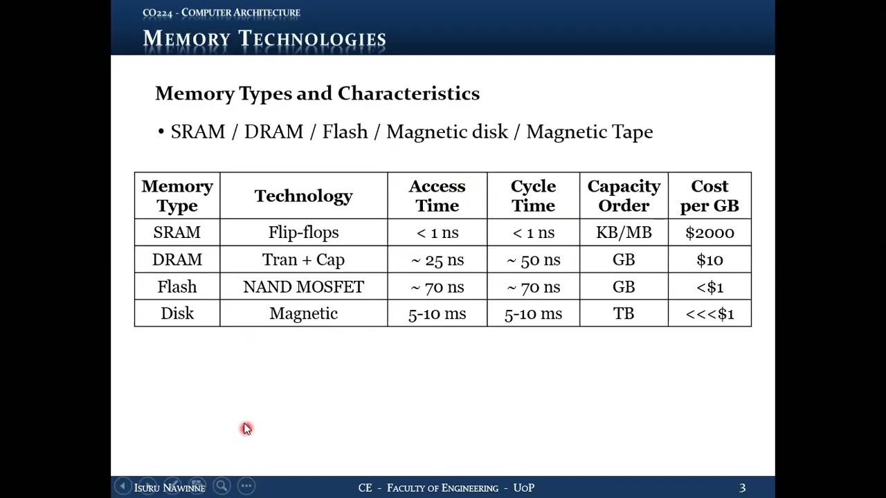
14.3 Memory Technologies: Types and Characteristics
14.3.1 Commonly Used Memory Technologies Today
- SRAM (Static RAM)
- DRAM (Dynamic RAM)
- Flash Memory
- Magnetic Disk
- Magnetic Tape
14.3.2 SRAM (Static RAM)
| Property | Value/Description |
|---|---|
| Technology | Built using flip-flops |
| Volatility | Volatile (loses content when power lost) |
| Access Time | Less than 1 nanosecond (< 1 ns) |
| Clock Frequency | More than 1 GHz |
| Cycle Time | Less than 1 nanosecond (< 1 ns) |
| Capacity | Kilobytes to Megabytes range |
| Cost | ~$2000 per gigabyte (VERY EXPENSIVE) |
| Speed | Extremely fast |
| Usage | Cache memories (small amounts due to cost) |
Note on Cycle Time:
- Cycle time = minimum time between two consecutive memory accesses
- Access time ≈ Cycle time for SRAM
14.3.3 DRAM (Dynamic RAM)
| Property | Value/Description |
|---|---|
| Technology | Transistors + Capacitors |
| Volatility | Volatile (requires power AND periodic refresh) |
| Access Time | ~25 nanoseconds (50 ns in some contexts) |
| Cycle Time | ~50 nanoseconds (double the access time) |
| Capacity | Gigabytes (8 GB, 16 GB, or more) |
| Cost | ~$10 per gigabyte |
| Usage | Main memory in computers |
Key Characteristics:
- Capacitor charge must be maintained
- "Destructive read": Reading loses the charge, requires rewrite/refresh
- Longer cycle time due to refresh requirement
- After reading, must rewrite data to same cell
- Significantly slower than SRAM (25-50 ns vs < 1 ns)
14.3.4 Flash Memory
| Property | Value/Description |
|---|---|
| Technology | NAND MOSFET (NAND gate with two gates) |
| Volatility | Non-volatile (retains data without power) |
| Access Time | ~70 nanoseconds |
| Cycle Time | ~70 nanoseconds |
| Capacity | Gigabytes range |
| Cost | Less than $1 per gigabyte |
| Usage | Secondary storage (SSDs - Solid State Devices/Drives) |
Limitation:
- Limited read/write cycles
- After several thousand cycles, memory cells may degrade
- Integrity decreases, capacity effectively decreases
- Slightly slower than DRAM, but non-volatile
14.3.5 Magnetic Disk
| Property | Value/Description |
|---|---|
| Technology | Magnetic (mechanical device) |
| Access Time | 5 to 10 milliseconds (MUCH slower than electronic memory!) |
| Cycle Time | Similar to access time (~5-10 ms) |
| Capacity | Several terabytes |
| Cost | Fraction of a dollar per gigabyte (very cheap) |
Usage:
- Previously: Main secondary storage
- Currently: Being replaced by flash/SSDs for secondary storage
- Now used primarily for tertiary storage, backups
- Good for long-term data retention, low cost
- Slowness acceptable for infrequent backup operations
14.4 The Memory Performance Problem
14.4.1 The CPU-Memory Speed Gap
CPU Clock Cycle:
- Modern CPUs: > 1 GHz clock frequency
- Clock cycle: < 1 nanosecond (1 ns corresponds to 1 GHz)
Main Memory (DRAM):
- Cycle time: ~50 nanoseconds
- Time between starts of two consecutive memory accesses: 50 ns
14.4.2 The Problem
Speed Discrepancy:
- CPU cycle: < 1 ns
- Memory cycle: 50 ns
- Memory is 50× SLOWER than CPU!
14.4.3 Impact on Pipelining
The Challenge:
- In MIPS pipeline, MEM stage must finish in ONE clock cycle
- Every pipeline stage must take same time
- How can MEM stage complete in 1 ns when memory takes 50 ns?
- Pipeline performance would be severely degraded
The Contradiction:
- CPU expects 1 ns memory access
- Actual DRAM takes 50 ns
- "Something is not right" - how can this work?
14.5 Memory Hierarchy Concept
14.5.1 The Solution: Memory Hierarchy
Core Idea:
- Trick the CPU into thinking memory is BOTH fast AND large
- Desired characteristics:
- Fast access times (like SRAM: < 1 ns)
- Large capacity (like Disk: terabytes)
- These characteristics don't exist in single technology
- Solution: Implement memory as a HIERARCHY
14.5.2 Memory Hierarchy Structure
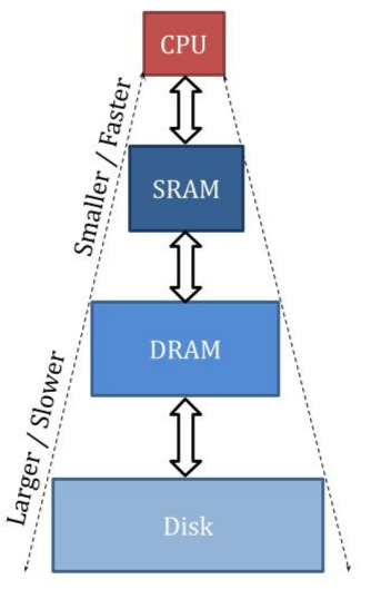
Memory Hierarchy with SRAM Cache, DRAM Main Memory, and Disk Storage
Level 1 (Top): SRAM (Cache)
- Smallest capacity
- Fastest speed
- Closest to CPU physically
Level 2: DRAM (Main Memory)
- Medium capacity
- Medium speed
Level 3 (Bottom): Disk
- Largest capacity
- Slowest speed
14.5.3 Key Principles
1. CPU Access Restriction
- CPU can ONLY access top level (SRAM cache)
- CPU thinks cache is the actual memory
- CPU cannot directly access DRAM or Disk
2. CPU's Perception
- Experiences the SPEED of SRAM
- Feels the CAPACITY of DRAM and Disk combined
- Illusion: Memory is as fast as SRAM AND as big as lowest level
3. Data Organization
- Upper levels contain SUBSET of data from lower levels
- SRAM (few MB) contains subset of DRAM (several GB)
- DRAM contains subset of Disk (several TB)
- At any given time, each level holds only a fraction of lower level's data
4. Hierarchy Characteristics
- Devices up the hierarchy: Smaller and faster
- Devices down the hierarchy: Larger but slower
14.5.4 The Challenge
What if CPU asks for data NOT in the cache (top level)?
- Need mechanism to copy data from lower levels
- This leads to the concepts of hits, misses, and cache management
14.6 Analogy: Music Library
14.6.1 Understanding Memory Hierarchy Through Music
Three-Level Music System
1. Mobile Phone (analogous to SRAM/Cache):
- Carries a subset of your favorite songs
- Always with you
- Listen to music directly from phone
- Limited storage (like cache has limited capacity)
2. Computer Hard Disk (analogous to DRAM/Main Memory):
- Main music collection stored here
- Larger collection than phone
- Not always accessible (not in pocket)
- Copy songs from here to phone when needed
3. Internet (analogous to Disk/Mass Storage):
- All songs available (massive storage)
- Download/buy songs from here
- Copy to computer, then to phone
14.6.2 Usage Scenarios
Scenario 1 (Hit)
- Want to listen to a song
- Song is already on phone
- Just play it directly
- Similar to cache hit: Data already in cache
Scenario 2 (Miss to Level 2)
- Want to listen to a song
- Song NOT on phone
- Must go to computer and copy to phone
- Then listen on phone
- Similar to cache miss: Must fetch from main memory
Scenario 3 (Miss to Level 3)
- Want to listen to a song
- Song NOT on phone AND NOT on computer
- Download from internet to computer
- Copy to phone
- Then listen
- Similar to cache miss to disk: Must fetch from lowest level
14.6.3 Key Parallels
- Always listen from phone (CPU always accesses cache)
- Main collection in computer (main memory holds primary data)
- All data available on internet (disk holds everything)
- Copy operations when data not available at higher levels
14.7 Memory Hierarchy Terminology
14.7.1 Essential Terms for Memory Access
HIT
Definition: Requested data IS available at the accessed level- CPU requests data → Data found in cache
- Like wanting to listen to song already on your phone
- Can be served immediately from that level
MISS
Definition: Requested data is NOT available at the accessed level- CPU requests data → Data NOT found in cache
- Like wanting to listen to song not on your phone
- Must fetch from lower level in hierarchy
HIT RATE
Definition: Ratio/percentage of accesses that result in hitsFormula:
Hit Rate = (Number of Hits) / (Total Accesses)
Example: 100 accesses, 90 hits → Hit Rate = 90% or 0.9
Indicates how often data is found at the accessed level. Higher hit rate = better performance.
MISS RATE
Definition: Ratio/percentage of accesses that result in missesFormula:
Miss Rate = (Number of Misses) / (Total Accesses)
Miss Rate = 1 - Hit Rate
Example: 100 accesses, 10 misses → Miss Rate = 10% or 0.1
Lower miss rate = better performance.
HIT LATENCY
Definition: Time taken to determine if access is a hit AND serve the data- Time to check if data is in cache and deliver it to CPU
- For SRAM cache: < 1 nanosecond
Components:
- Time to search cache
- Time to verify data presence
- Time to extract and send data to CPU
MISS PENALTY
Definition: EXTRA time required when access is a missProcess:
- Determine it's a miss (hit latency spent)
- Go to next level (DRAM)
- Find the data
- Copy to cache
- Put in appropriate place
- Deliver to CPU
Key Points:
- Total time on miss = Hit Latency + Miss Penalty
- Miss penalty for DRAM access can be 100× hit latency
- Very expensive in terms of time!
14.8 Performance Impact and Requirements
14.8.1 Average Memory Access Time
Formula:
Average Access Time = Hit Latency + (Miss Rate × Miss Penalty)
Explanation:
- ALL accesses consume hit latency (must check cache)
- Only misses consume additional miss penalty
- Miss Rate determines portion of accesses incurring penalty
14.8.2 Example Analysis
Given:
- Hit Latency (SRAM): < 1 nanosecond
- Miss Penalty (DRAM access): ~100 nanoseconds (100× slower)
- CPU clock cycle: < 1 nanosecond
For Pipeline to Work
- MEM stage must complete in 1 clock cycle
- Memory access must complete in < 1 ns most of the time
Required Hit Rate Calculation
If Hit Rate = 99.9% (Miss Rate = 0.1%):
Average Time = 1 ns + (0.001 × 100 ns)
             = 1 ns + 0.1 ns
             = 1.1 ns
Still close to 1 clock cycle!
If Hit Rate = 90% (Miss Rate = 10%):
Average Time = 1 ns + (0.10 × 100 ns)
             = 1 ns + 10 ns
             = 11 ns
Unacceptable! 11× slower than CPU clock!
14.8.3 Critical Requirement
- Need VERY HIGH hit rate at cache level
- Not just high, but VERY, VERY high
- Target: 99.9% or better
- Only 0.1% of accesses should go to memory
14.8.4 Performance Implications
With 99.9% Hit Rate
- 99.9% of time: CPU works fine, memory appears fast
- 0.1% of time: CPU must STALL, wait for data from DRAM
- Stall is unavoidable for misses
- Overall: CPU maintains illusion of fast, large memory
With Lower Hit Rate
- More frequent stalls
- Pipeline performance degrades significantly
- Average memory access time increases
- CPU slows down dramatically
Conclusion:
- Must ensure VERY high hit rate at SRAM level
- Memory hierarchy only works if locality principles hold
- Like having most songs you want to listen to already on phone
- Don't want to copy from computer frequently (time-consuming)
14.9 Principles of Locality
14.9.1 Foundation for Memory Hierarchy Success
Nature of Computer Programs:
- Programs access only SMALL portion of entire address space at any given time
- Address space: Entire memory range (address 0 to maximum address)
- At any time window, program uses only small fraction of total data
- True by nature of how programs are written, compiled, and executed
- True for instruction sets like ARM, MIPS
14.9.2 Temporal Locality (Locality in Time)
Definition
"Recently accessed data are likely to be accessed again soon"
Explanation:
- If you access memory address A at time T
- High probability of accessing address A again at time T+ΔT (soon after)
- Same data accessed multiple times in short time window
- "Locality in time" - data clustered temporally
Common Examples in Programs
a) Loop Index Variables:
for (int i = 0; i < 100; i++) {
    // i is accessed every iteration
    // Same memory location for 'i' accessed repeatedly
}
b) Loop-Invariant Data:
for (int i = 0; i < n; i++) {
    result = result + array[i] * constant;
    // 'result' and 'constant' accessed every iteration
}
c) Function/Procedure Calls:
- Local variables accessed multiple times during function execution
- Same stack frame locations accessed repeatedly
d) Instructions:
- Loop body instructions executed many times
- Same instruction addresses accessed repeatedly
Music Analogy
- If you listen to a song, you're likely to listen to it again soon
- Sometimes listen to same song 10 times in a row
- Want to replay favorite songs
Degree of Temporal Locality
- Varies from program to program
- But present in nearly ALL programs
- Stronger in some (tight loops) than others
14.9.3 Spatial Locality (Locality in Space)
Definition
"Data located close to recently accessed data are likely to be accessed soon"
Explanation:
- If you access memory address A at time T
- High probability of accessing addresses A+1, A+2, A+3, ... soon after
- Sequential or nearby addresses accessed together
- "Locality in space" - data clustered spatially in memory
Common Examples in Programs
a) Array Traversal:
for (int i = 0; i < 100; i++) {
    sum += array[i];
    // Access array[0], then array[1], then array[2], ...
    // Sequential memory addresses
}
b) Sequential Instruction Execution:
- Instructions stored sequentially in memory
- PC increments: fetch instruction at PC, then PC+4, then PC+8, ...
- Except for branches, mostly sequential
c) Data Structures:
struct Student {
    int id;
    char name[50];
    float gpa;
};
Student s;
// Accessing s.id, then s.name, then s.gpa
// Nearby memory locations
d) String Processing:
char str[] = "Hello";
for (int i = 0; str[i] != '\0'; i++) {
    // Access str[0], str[1], str[2], ...
    // Consecutive bytes in memory
}
Music Analogy
- If you listen to song by artist X, likely to listen to another song by artist X
- If you listen to song from album Y, likely to listen to next song in album Y
- Related/nearby songs accessed together
Degree of Spatial Locality
- Varies by data access patterns
- Strong in array-based algorithms
- Present in most structured programs
14.9.4 Universal Applicability
- Both principles hold true for NEARLY ALL programs
- Degree varies, but principles universally applicable
- Foundation assumptions for cache design
14.10 Cache Memory Concept and Block-Based Operation
14.10.1 Cache Memory Overview
Purpose:
- Memory device at top level of hierarchy
- Based on two principles of locality
- Decides what data to keep based on locality principles
14.10.2 Data Organization: BLOCKS
Key Concepts:
- CPU requests individual WORDS from memory
- Between cache and memory: Handle BLOCKS of data
- Block = multiple consecutive words
- Block size example: 8 bytes = 2 words (with 4-byte words)
- Hidden from CPU (CPU still thinks in words)
14.10.3 Why Blocks? (Spatial Locality)
Instead of Words
- Fetch single word CPU requested
- Next access likely nearby address
- Would require another fetch
Using Blocks
- Fetch requested word AND nearby words together
- Bring entire block (e.g., 8 consecutive bytes)
- Subsequent accesses likely in same block (spatial locality)
- Reduces future misses
Music Library Analogy
- Want to listen to one song → Copy entire album to phone
- Not just the single song you want right now
- Because you'll likely want other songs from same album soon
- Saves future copy operations
Block Benefits
- Exploits spatial locality
- Reduces miss rate
- Amortizes fetch cost over multiple words
- More efficient use of memory bandwidth
14.10.4 Cache Management Decisions
1. What to Keep in Cache
- Based on BOTH locality principles
- Recently accessed data (temporal locality)
- Blocks containing nearby data (spatial locality)
2. What to Evict from Cache
- Based on TEMPORAL locality
- When cache full and need space for new block
- Must throw out existing data
14.10.5 Eviction Strategy (Ideal)
Least Recently Used (LRU):
- Throw out LEAST RECENTLY USED (LRU) data
- If cache has 10 blocks, need to evict 1
- Choose the block that was used longest time ago
- Keep more recently used blocks
- Temporal locality suggests LRU block least likely to be accessed soon
Example:
- Cache has blocks A, B, C, D, E
- Last access times: A(10 cycles ago), B(2 cycles ago), C(50 cycles ago), D(5 cycles ago), E(1 cycle ago)
- Need to evict one block
- Evict C (least recently used, 50 cycles ago)
- Keep E, B, D, A (more recently used)
14.11 Memory Addressing: Bytes, Words, and Blocks
14.11.1 Byte Address
Definition: Address referring to individual byte in memoryCharacteristics:
- Each byte-sized location has unique address
- Standard memory addressing
- Address Space: With 32-bit address, can access 2³² individual bytes
Example Address:
Address: 00000000000000000000000000001010 (binary)
       = 10 (decimal)
Points to: Byte at memory location 10
Memory Structure:
Address 0:  [byte 0]
Address 1:  [byte 1]
Address 2:  [byte 2]
...
Address 10: [byte 10]  ← This byte addressed by example
...
14.11.2 Word Address
Definition: Address referring to a word (multiple bytes) in memory Typical Word Size: 4 bytes (32 bits)Word Alignment
- Words start at addresses that are multiples of 4
- Word 0: Addresses 0, 1, 2, 3
- Word 1: Addresses 4, 5, 6, 7
- Word 2: Addresses 8, 9, 10, 11
- Word 3: Addresses 12, 13, 14, 15
Word Address Format (32-bit)
[30-bit word identifier][2-bit byte offset]
                         └── Always "00" for word-aligned addresses
Example:
Address: ...00001000 (binary)
- Last 2 bits: 00 → Word-aligned
- Remaining bits: Identify which word
- This is address 8, start of word 2
Byte Within Word
Last 2 bits select byte within word:
00→ First byte (address 8)01→ Second byte (address 9)10→ Third byte (address 10)11→ Fourth byte (address 11)
Key Points:
- Word addresses are multiples of 4
- Can divide by 4 without remainder
- Last 2 bits = 00 for word addresses
- NOT all addresses ending in 00 are word addresses, but word addresses end in 00
- Only portion of address except last 2 bits identifies the word
14.11.3 Block Address
Definition: Address referring to a block (multiple words) in memory Example Block Size: 8 bytes = 2 wordsBlock Alignment
- Blocks start at addresses that are multiples of 8
- Block 0: Addresses 0-7
- Block 1: Addresses 8-15
- Block 2: Addresses 16-23
- Block 3: Addresses 24-31
Block Address Format (32-bit)
[Block Identifier][3-bit offset]
                   └── Last 3 bits for 8-byte blocks
Example:
Address: 00000000000000000000000000101101 (binary)
       = 45 (decimal)

Block Address Portion:
- Ignore last 3 bits: 101 (offset part)
- Block address: 00000000000000000000000000101 (identifies block)
- This identifies the block containing address 45
Offset Within Block (3 bits for 8-byte blocks)
Offset Within Block (3 bits for 8-byte blocks)
BYTE OFFSET (all 3 bits):
Used to identify individual BYTE within block:
000→ Byte 0001→ Byte 1- ...
111→ Byte 7
WORD OFFSET (most significant bit of offset):
Used to identify WORD within block (when block has 2 words):
0XX→ First word (bytes 0-3)1XX→ Second word (bytes 4-7)- Only need 1 bit to select between 2 words
14.11.4 Address Components Summary
For address with 8-byte blocks, 4-byte words:
[Block Address][Word Offset][Byte in Word]
  ^              ^              ^
  |              |              └── 2 bits: Select byte within word
  |              └── 1 bit: Select word within block
  └── Remaining bits: Identify which block
Example Breakdown:
Address: ...00101101
- Last 2 bits (01): Byte offset within word → Byte 1 of word
- 3rd bit from right (1): Word offset → Second word of block
- Remaining bits (...00101): Block address → Block 5
All Bytes in Same Block:
- Share same block address
- Differ only in offset bits
Important Distinctions:
- Byte address: Full 32 bits
- Word address: Term refers to full address of word-aligned location
- Block address: Term refers to portion of address identifying block (excluding offset)
14.12 The Cache Addressing Problem
14.12.1 Problem Statement
In Main Memory
- Direct addressing: Address 10 → Direct access to location 10
- Like array indexing: array[10] directly accesses index 10
- Straightforward: Address uniquely identifies memory location
- No search required: Hardware directly decodes address
In Cache
- Cache is MUCH smaller than memory
- Memory: Gigabytes (millions/billions of addresses)
- Cache: Kilobytes or Megabytes (thousands/few million bytes)
- Example: Memory has 1 million addresses, cache has only 8 slots
14.12.2 The Challenge
- CPU generates address from full address space (e.g., address 10)
- Cache has only 8 slots (indices 0-7)
- Cannot directly use memory address as cache index
- Address 10 doesn't directly map to cache location
- How to find data in cache with memory address?
14.12.3 Initial Solution Idea: Store Addresses with Data
Approach:
- Store memory address alongside data in cache
- Each cache entry: [Address | Data]
- When CPU requests address, search cache for matching address
Problems with This Approach:
1. Space Overhead:
- Must store full address (e.g., 32 bits) with each data block
- Significant storage overhead
- Example: 32-bit address + 256-bit data block = ~13% overhead
2. Search Time:
- Must search through ALL cache entries
- Sequential or parallel search required
- Example: 8 cache slots → Check all 8 tags
- Time-consuming, degrades hit latency
- Cannot directly access cache entry
14.12.4 Need for Better Solution
Requirements:
- Require MAPPING between memory addresses and cache locations
- Want DIRECT access (no search) if possible
- Must be efficient in both space and time
Requirements for Practical Cache:
- Fast access (< 1 ns hit latency)
- Minimal storage overhead
- Direct or near-direct cache indexing
- Efficient tag comparison (if needed)
Solution Preview: Address Mapping Functions
- Need function: Memory Address → Cache Location
- Different mapping strategies possible
- Simplest: Direct Mapping (discussed next)
14.13 Direct-Mapped Cache
14.13.1 Direct Mapping Concept
Definition:
- Each memory address maps to EXACTLY ONE cache location
- One-to-one deterministic mapping
- No choice in cache placement
Mapping Rule:
Cache Index = Block Address MOD (Number of Blocks in Cache)
Formula:
Cache Index = (Block Address) mod (Cache Size in Blocks)
Example:
- Cache has 8 blocks → Indices 0-7
- Block address = 13
- Cache index = 13 mod 8 = 5
- Block 13 maps ONLY to cache index 5
14.13.2 Mathematical Properties
Mod Operation with Powers of 2
- Cache sizes typically powers of 2 (1, 2, 4, 8, 16, 32, ...)
- Mod by power of 2 = take least significant bits
- Example: N mod 8 = N mod 2³ = last 3 bits of N
Hardware Implementation
- No division circuit needed!
- Simply extract least significant bits
- Very fast, pure combinational logic
14.13.3 Direct Mapping Example
Given:
- Block size: 8 bytes
- Cache size: 8 blocks
- Cache indices: 0, 1, 2, 3, 4, 5, 6, 7
Cache Structure (Initial View):
| Index | Data Block |
|---|---|
| 0 | [64 bits] |
| 1 | [64 bits] |
| 2 | [64 bits] |
| 3 | [64 bits] |
| 4 | [64 bits] |
| 5 | [64 bits] |
| 6 | [64 bits] |
| 7 | [64 bits] |
Example Addresses:
Address 1:
Binary: ...00000001[011]
        └─ Block address = 0
        └─ Offset = 3 bytes
Cache index = 0 mod 8 = 0
Maps to cache index 0
Address 2 (block address in focus):
Binary: ...00000101[000]
        └─ Block address = 5
        └─ Offset = 0
Cache index = 5 mod 8 = 5
Maps to cache index 5
14.13.4 Address Structure for Direct-Mapped Cache
[Tag][Index][Offset]
  ^     ^       ^
  |     |       └── Identifies byte/word within block
  |     └── Identifies cache location (index)
  └── Remaining bits to differentiate blocks mapping to same index
Bit Allocation (for 8-block cache, 8-byte blocks, 32-bit address)
- Offset: 3 bits (for 8-byte blocks: 2³ = 8)
- Index: 3 bits (for 8 cache blocks: 2³ = 8)
- Tag: 26 bits (remaining: 32 - 3 - 3 = 26)
Index Bits
- Least significant bits of block address
- Directly select cache location
- Number of bits = log₂(cache blocks)
- 8 blocks → 3 index bits
- 16 blocks → 4 index bits
- 32 blocks → 5 index bits
14.14 The Tag Problem in Direct-Mapped Cache
14.14.1 Conflict Issue
Multiple Blocks → Same Index:
- Many memory blocks map to same cache index
- Example: Blocks 5, 13, 21, 29, ... all map to index 5 (mod 8)
- Only ONE can occupy cache index 5 at a time
Example Addresses Mapping to Index 5:
Address A:
Block address: ...00000101
Index bits (last 3): 101 → Index 5
Address B:
Block address: ...00001101
Index bits (last 3): 101 → Index 5
Both map to index 5, but different blocks!
14.14.2 The Problem
- When CPU requests address with index 5
- Is data at index 5 for Address A or Address B?
- Need way to differentiate between conflicting blocks
14.14.3 Solution: TAG FIELD
Tag Definition:
- Remaining bits of block address (excluding index and offset)
- Stored WITH data in cache
- Used to verify correct block is present
Tag = Block Address (excluding index bits)
Example Address Breakdown
Full Address:
[26-bit Tag][3-bit Index][3-bit Offset]
Address A
Binary representation:
00000000000000000000000000 101 000
| Field | Bits (binary) | Decimal |
|---|---|---|
| Tag | 00000000000000000000000000 (26 bits) | 0 |
| Index | 101 | 5 |
| Offset | 000 | 0 |
Address B
Binary representation:
00000000000000000000000001 101 000
| Field | Bits (binary) | Decimal |
|---|---|---|
| Tag | 00000000000000000000000001 (26 bits) | 1 |
| Index | 101 | 5 |
| Offset | 000 | 0 |
Both addresses map to cache index 5 but have different tag values (0 vs 1), so they refer to different memory blocks that conflict at the same cache index.
14.14.4 Cache Structure with Tags
| Index | Valid | Tag | Data Block |
|---|---|---|---|
| 0 | V | Tag0 | [64 bits] |
| 1 | V | Tag1 | [64 bits] |
| 2 | V | Tag2 | [64 bits] |
| 3 | V | Tag3 | [64 bits] |
| 4 | V | Tag4 | [64 bits] |
| 5 | V | Tag5 | [64 bits] |
| 6 | V | Tag6 | [64 bits] |
| 7 | V | Tag7 | [64 bits] |
Storage Requirements Per Cache Entry:
- Tag: 26 bits (in this example)
- Valid bit: 1 bit
- Data: 64 bits (8 bytes)
- Total: 91 bits per entry
Storage Overhead:
Overhead = (Tag + Valid) / Total
         = (26 + 1) / (26 + 1 + 64)
         = 27 / 91
         ≈ 30% overhead in this small example
Note on Overhead
- Example uses VERY small cache (8 blocks)
- Real caches are much larger (thousands of blocks)
- Larger caches → More index bits
- More index bits → Fewer tag bits
- Overhead percentage decreases with larger caches
Example with Larger Cache:
- 1024 blocks (2¹⁰)
- Index: 10 bits
- Tag: 32 - 10 - 3 = 19 bits
- Overhead: (19+1)/84 ≈ 24% (better)
14.14.5 Valid Bit
Purpose:
- Indicates whether cache entry contains valid data
- Prevents using uninitialized/stale data
Initial State:
- At program start, cache is empty
- All entries contain garbage/random values
- All valid bits set to 0 (invalid)
After Data Loaded:
- When block loaded into cache, valid bit set to 1
- Indicates data is reliable
Uses Beyond Initialization:
- Cache coherence (multi-processor systems)
- Invalidating stale data
- Handling context switches
14.15 Cache Read Access Operation
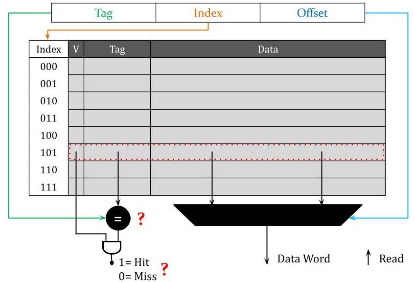
Direct-Mapped Cache Read Access Process
14.15.1 Read Access Process
CPU Provides:
- Address (word or byte address)
- Control Signal: Read/Write indicator (from control unit)
14.15.2 For Read Access
Step 1: ADDRESS BREAKDOWN
Process:
- Receive address from CPU
- Parse into three fields:
- Tag bits
- Index bits
- Offset bits
Example Address (32-bit):
[26-bit Tag][3-bit Index][3-bit Offset]
Step 2: INDEXING THE CACHE
- Extract index bits from address
- Use index to directly access cache entry
- Combinational logic routes to correct entry
- Like array indexing: index 5 → entry 5
- No search needed!
- Fast: Pure combinational delay
Hardware:
- Decoder circuit takes index bits
- Selects one of N cache entries
- Activates corresponding row
Step 3: TAG COMPARISON
- Extract stored tag from selected cache entry
- Extract tag bits from incoming address
- Compare the two tags
- Use comparator circuit
Comparator Circuit:
- For each bit position: XNOR gate
- XNOR outputs 1 if bits match, 0 if different
- AND all XNOR outputs together
- Final output: 1 if all bits match (tags equal), 0 otherwise
Example (4-bit tags):
Stored tag:   1 0 1 1
Address tag:  1 0 1 1
XNOR:         1 1 1 1  → AND = 1 (MATCH!)

Stored tag:   1 0 1 1
Address tag:  1 0 0 1
XNOR:         1 1 0 1  → AND = 0 (NO MATCH)
For N-bit tag:
- N XNOR gates (parallel)
- 1 N-input AND gate
- Very fast combinational circuit
Step 4: VALID BIT CHECK
- Extract valid bit from selected cache entry
- Check if entry is valid
- Valid bit = 1 → Entry contains valid data
- Valid bit = 0 → Entry is invalid (ignore)
Step 5: HIT/MISS DETERMINATION
- Combine tag comparison and valid bit
- Hit = (Tag Match) AND (Valid Bit = 1)
- Miss = (Tag Mismatch) OR (Valid Bit = 0)
Logic Circuit:
Tag Match Output ─┐
                   AND ─→ Hit/Miss Signal
Valid Bit ────────┘
Output:
- 1 → HIT (data present and valid)
- 0 → MISS (data not present or invalid)
Hit Latency:
Time for steps 2-5, dominated by:
- Indexing combinational delay
- Tag comparator delay
- Valid bit access
- Typically < 1 nanosecond for SRAM
Step 6: DATA EXTRACTION (Parallel with Tag Check)
- Can happen in PARALLEL with tag comparison
- Extract entire data block from selected cache entry
- Put data block on internal wires
Data Block:
- Contains multiple words
- Example: 8 bytes = 2 words (4 bytes each)
Step 7: WORD SELECTION (Using Offset)
- CPU wants a single WORD, not entire block
- Use offset bits to select correct word from block
- Offset bits → Multiplexer select signal
Multiplexer (MUX):
- Inputs: All words in the data block
- Select: Word offset bits from address
- Output: Selected word
Example (2 words per block):
- Block contains: Word0 (bytes 0-3), Word1 (bytes 4-7)
- Word offset = 0 → Select Word0
- Word offset = 1 → Select Word1
- Need 1-bit select for 2:1 MUX
Example (4 words per block):
- Block contains: Word0, Word1, Word2, Word3
- Word offset = 2 bits → Select among 4 words
- Need 4:1 MUX
Timing:
- Data extraction and word selection happen in parallel with tag check
- Both combinational circuits
- Similar delays
- Can overlap operations
Step 8: DECISION BASED ON HIT/MISS
If HIT (signal = 1):
- Selected word is correct data
- Send word to CPU immediately
- Access complete
- Total time: Hit latency (< 1 ns)
If MISS (signal = 0):
- Selected word is WRONG data (different block or invalid)
- CANNOT send to CPU
- Must fetch correct block from main memory (DRAM)
- CPU must STALL (wait)
- Cache controller takes over
- Total time: Hit latency + Miss penalty
Miss Handling:
- Will discuss in next lecture
- Involves accessing main memory
- Bringing block into cache
- Potentially evicting old block
- Then serving CPU request
14.16 Cache Circuit Components Summary
14.16.1 Key Circuit Elements
1. INDEXING CIRCUITRY
- Input: Index bits from address
- Function: Decoder to select cache entry
- Output: Activates one cache row
- Type: Combinational logic
- Delay: Part of hit latency
2. TAG COMPARATOR
- Input: Stored tag, Address tag
- Function: Multi-bit equality check
- Components:
- N XNOR gates (N = tag bit width)
- 1 N-input AND gate
- Output: 1 if equal, 0 if not equal
- Type: Combinational logic
- Delay: Part of hit latency
3. VALID BIT CHECK
- Input: Valid bit from cache entry
- Function: Read and check validity
- Output: 1 if valid, 0 if invalid
- Type: Simple wire/buffer
- Delay: Minimal
4. HIT/MISS LOGIC
- Input: Tag match signal, Valid bit
- Function: AND gate
- Output: Hit/Miss signal
- Type: Combinational logic
- Delay: Single gate delay
5. DATA ARRAY ACCESS
- Input: Index bits
- Function: Read data block from cache
- Output: Multi-word data block
- Type: SRAM memory read
- Delay: SRAM access time (parallel with tag check)
6. WORD SELECTOR (Multiplexer)
- Input: Data block, Word offset bits
- Function: Select one word from block
- Output: Single word
- Type: MUX (combinational)
- Delay: MUX delay (parallel with tag check)
7. CONTROL LOGIC (Cache Controller)
- Input: Hit/Miss signal, Read/Write control
- Function: Decide next actions
- Output: Control signals for CPU, memory
- On Hit: Enable data to CPU
- On Miss: Initiate memory fetch, stall CPU
- Type: Sequential logic (state machine)
14.16.2 Hit Latency Components
Contributing Factors:
- Indexing delay
- Tag comparison delay
- Valid bit check delay
- Hit/Miss determination delay
- Word selection delay (parallel)
- Wire delays
Dominant Delays:
- Indexing (decoder)
- Tag comparator (XNOR + AND)
- These determine critical path
Parallelism:
- Tag check and data extraction happen simultaneously
- Reduces total hit latency
- Only one path delay counts (whichever is longer)
14.17 Next Lecture Preview
14.17.1 Topics to Cover
1. Cache Miss Handling
- What happens after miss is determined?
- How to fetch block from main memory?
- Where to place new block in cache?
- What to do if cache location occupied?
2. Cache Controller State Machine
- Not just combinational logic
- Sequential control needed for misses
- Multiple clock cycles to handle miss
- States: Idle, Compare Tags, Allocate, Write Back, etc.
3. Write Operations
- Read operation covered this lecture
- Write more complex: Must update cache AND memory
- Write policies: Write-through, Write-back
- Dirty bits for modified blocks
4. Replacement Policies
- When cache full, which block to evict?
- Least Recently Used (LRU)
- Other policies: FIFO, Random, LFU
5. Performance Analysis
- Calculate average access time
- Impact of hit rate, miss penalty
- Cache size vs. performance tradeoffs
6. Advanced Cache Concepts
- Set-associative caches (beyond direct-mapped)
- Multi-level caches (L1, L2, L3)
- Fully associative caches
14.18 Key Takeaways and Summary
14.18.1 Historical Foundations
- Early computers had no memory/software concept
- Alan Turing conceived stored program computer (1936)
- John von Neumann implemented it in EDVAC (1948)
- Von Neumann architecture: Unified memory for instructions and data
- Harvard architecture: Separate instruction and data memories
14.18.2 Memory Technologies Hierarchy
| Technology | Speed | Size | Cost |
|---|---|---|---|
| SRAM | Fastest (< 1 ns) | Smallest (KB-MB) | Most expensive ($2000/GB) |
| DRAM | Medium (~50 ns) | Medium (GB) | Moderate ($10/GB) |
| Flash | Similar to DRAM | Gigabytes | Cheap (< $1/GB) |
| Disk | Slowest (5-10 ms) | Largest (TB) | Cheapest (cents/GB) |
14.18.3 The Performance Problem
- CPU cycle time: < 1 nanosecond
- Main memory cycle time: ~50 nanoseconds
- Memory 50× slower than CPU!
- Pipeline requires memory access in 1 cycle
- Cannot directly use DRAM for CPU memory accesses
14.18.4 Memory Hierarchy Solution
- Multiple levels: SRAM (cache) → DRAM → Disk
- CPU accesses only top level (cache)
- Upper levels hold subsets of lower levels
- Trick CPU: Fast as SRAM, large as Disk
- Requires very high hit rate (> 99.9%) at cache level
14.18.5 Principles of Locality
1. Temporal Locality: Recently accessed data likely accessed again soon
- Example: Loop variables, instructions in loops
2. Spatial Locality: Data near recently accessed data likely accessed soon
- Example: Array elements, sequential instructions
- Both principles present in virtually all programs
- Foundation for cache effectiveness
14.18.6 Memory Addressing
- Byte Address: Individual byte reference (full address)
- Word Address: 4-byte word reference (last 2 bits = 00 for alignment)
- Block Address: Multiple-word block reference (excludes offset bits)
- Address structure: [Block Address][Offset]
- Offset subdivides: [Word Offset][Byte in Word]
14.18.7 Cache Terminology
- Hit: Data found in cache → Fast access (< 1 ns)
- Miss: Data not in cache → Slow access (+ ~100 ns penalty)
- Hit Rate: Fraction of accesses that hit (want > 99.9%)
- Miss Rate: Fraction of accesses that miss (1 - Hit Rate)
- Hit Latency: Time to determine hit and access data
- Miss Penalty: EXTRA time to fetch from memory on miss
14.18.8 Cache Organization (Direct-Mapped)
- Each memory block maps to exactly ONE cache location
- Mapping: Cache Index = Block Address mod (Cache Size)
- Address fields: [Tag][Index][Offset]
- Index: Selects cache entry directly (no search!)
- Tag: Differentiates blocks mapping to same index
- Offset: Selects word/byte within block
- Valid bit: Indicates if entry contains valid data
14.18.9 Direct-Mapped Cache Structure
- Tag array: Stores tags for verification
- Valid bit array: Validity indicators
- Data array: Stores actual data blocks
- Index not stored (implicit in position)
14.18.10 Cache Read Access Process
- Extract index from address → Access cache entry
- Extract tag from cache entry → Compare with address tag
- Check valid bit from entry
- Determine hit/miss: (Tag Match) AND (Valid)
- In parallel: Extract data block, select word using offset
- If HIT: Send word to CPU (done in < 1 ns)
- If MISS: Must fetch from memory (will cover next lecture)
14.18.11 Critical Requirements
- Hit latency must be < 1 CPU clock cycle
- Hit rate must be very high (> 99.9%)
- Only way to achieve: Exploit locality principles
- Direct mapping enables fast indexing (no search)
- Parallel tag check and data extraction minimize latency
14.18.12 Average Access Time Formula
Average Access Time = Hit Latency + (Miss Rate × Miss Penalty)
- Must keep Miss Rate very low for performance
- Even 1% miss rate catastrophic if penalty is 100×
- Example: 1% miss rate → 1 + (0.01 × 100) = 2 ns average
- Example: 0.1% miss rate → 1 + (0.001 × 100) = 1.1 ns average
- Target: 99.9% or better hit rate
14.18.13 Pending Topics (Next Lectures)
- Cache miss handling and memory fetch
- Cache controller state machine
- Write operations and write policies
- Block replacement strategies (LRU, etc.)
- Set-associative and fully associative caches
- Multi-level cache hierarchies
- Performance analysis and optimization
14.18.14 Music Library Analogy Summary
- Phone (cache): Small, fast, always accessible
- Computer (main memory): Larger, slower, main collection
- Internet (disk): Huge, slowest, everything available
- Listen from phone (CPU accesses cache)
- Copy from computer when song not on phone (fetch on miss)
- Download from internet when not on computer (fetch from disk)
- Keep favorite songs on phone (exploit temporal locality)
- Copy whole album at once (exploit spatial locality)
Key Takeaways
- Stored-program concept revolutionized computing—programs stored in memory like data, eliminating manual reconfiguration for each algorithm.
- Von Neumann architecture established fundamental computer organization—CPU, memory, and I/O with instructions and data sharing same memory.
- Processor-memory speed gap creates performance bottleneck—CPU operates at nanosecond scale while main memory requires tens of nanoseconds.
- Memory hierarchy provides illusion of large, fast memory—small fast cache near CPU, larger slower DRAM main memory, massive slow disk storage.
- Temporal locality: Recently accessed data likely accessed again soon—programs exhibit loops, function calls, and repeated variable access patterns.
- Spatial locality: Nearby data likely accessed soon—programs access arrays sequentially and instructions execute in order.
- Cache exploits locality to achieve high hit rates—keeping frequently accessed data in fast storage dramatically improves average access time.
- Cache organized in blocks, not individual words—exploiting spatial locality by fetching multiple words together.
- Direct-mapped cache: Each memory block maps to exactly one cache location—simplest cache organization using modulo arithmetic for mapping.
- Address breakdown: Tag + Index + Offset—index selects cache entry, tag identifies specific block, offset selects word within block.
- Valid bit indicates cache entry contains meaningful data—essential for distinguishing real data from uninitialized entries at startup.
- Cache hit occurs when requested data found in cache—CPU receives data in ~1 nanosecond, avoiding slow main memory access.
- Cache miss requires main memory fetch—takes ~100 nanoseconds, replacing cache entry with new block from memory.
- Hit rate determines cache effectiveness—even 1% miss rate significantly impacts average memory access time with 100× penalty.
- Block size affects performance—larger blocks exploit spatial locality better but reduce total number of blocks, potentially increasing conflicts.
- Cache size represents total data storage capacity—typical L1 caches 32-64 KB, L2 caches 256 KB-1 MB.
- Tag comparison happens in parallel with data access—enabling fast hit detection and maintaining single-cycle cache access.
- Music library analogy clarifies cache concept—phone (cache) holds favorites, computer (DRAM) has main collection, internet (disk) contains everything.
- Cache transparent to programmer—software sees uniform memory, hardware manages cache automatically for best performance.
- Memory hierarchy only works because programs exhibit locality—without temporal and spatial locality, caching would fail catastrophically.
Summary
The introduction to memory systems and cache memory reveals how the fundamental processor-memory speed gap—with CPUs operating 100× faster than main memory—drives sophisticated cache hierarchy designs that create the illusion of large, fast memory. Historical context from Alan Turing's theoretical foundations through Von Neumann's stored-program architecture establishes how modern computers execute instructions fetched from memory rather than requiring manual reconfiguration. The memory hierarchy concept, with small fast SRAM caches near the CPU, larger slower DRAM main memory, and massive disk storage, exploits two fundamental program properties: temporal locality (recently accessed data likely accessed again soon) and spatial locality (nearby data likely accessed soon). Cache memory, organized in blocks rather than individual words, dramatically improves average access time by maintaining frequently accessed data in fast storage, achieving hit rates often exceeding 95% in practice. Direct-mapped cache organization, the simplest mapping scheme, uses modulo arithmetic to assign each memory block to exactly one cache location, with address bits divided into tag (identifying specific block), index (selecting cache entry), and offset (choosing word within block). The valid bit distinguishes real cached data from uninitialized entries, essential at system startup when cache contains random values. Cache hits deliver data in approximately 1 nanosecond while misses require ~100 nanosecond main memory access, making even small miss rates significant—a 1% miss rate doubles average access time from 1 ns to 2 ns. The music library analogy effectively clarifies concepts: phone storage represents cache (small, fast, always accessible), computer storage represents main memory (larger, slower, main collection), and internet streaming represents disk (unlimited, very slow, backup). This cache transparency—programmer sees uniform memory while hardware automatically manages caching—enables software compatibility across different cache configurations. The critical insight remains that memory hierarchy effectiveness depends entirely on programs exhibiting locality; without these natural access patterns inherent to how we write code, caching would provide no benefit. Understanding cache fundamentals proves essential for both hardware designers optimizing cache architectures and software developers writing cache-friendly code that maximizes hit rates.