Click the thumbnail above to watch the video lecture on YouTube
15.1 Introduction
This lecture provides a comprehensive, step‑by‑step examination of how a direct‑mapped cache services read and write requests, differentiates hits from misses, and preserves data correctness. We finish the full read path (including stall + block fetch sequence), analyze write hits and misses, and introduce the write‑through policy as the simplest consistency mechanism between cache and main memory. Performance consequences of constant memory writes, the need for high hit rates, and the motivation for more advanced write‑back policies (next lecture) are emphasized. By the end you will understand exactly what the cache controller must do (state transitions, signals, data/tag/valid updates) for every access type and why write policies are a central architectural tradeoff.
15.2 Lecture Introduction and Recap
15.2.1 Previous Lecture Review
Memory Systems Foundation
- Memory hierarchy concept (SRAM → DRAM → Disk)
- Illusion of large and fast memory simultaneously
- CPU accesses only cache (top level)
Locality Principles
- Temporal locality: Recently accessed data likely accessed again soon
- Spatial locality: Nearby data likely accessed soon
- Foundation for cache effectiveness
Direct-Mapped Cache Introduction
- Each memory block maps to exactly ONE cache location
- Mapping function: Cache Index = Block Address MOD Cache Size
- Read access process partially covered
Cache Structure (Recap)
- Data array: Stores data blocks (not individual words)
- Tag array: Stores tags for block identification
- Valid bit array: Indicates valid/invalid entries
- Index: Not stored, implicit in position (for convenience in diagrams)
Address Breakdown (Recap)
[Tag][Index][Offset]
^      ^       ^
|      |       └── Identifies word/byte within block
|      └── Identifies cache entry (direct mapping)
└── Remaining bits for block identification
15.2.2 Today's Focus
- Complete discussion of read miss handling
- Write access operations (hit and miss)
- Write policies and their implications
- Data consistency issues
- Performance considerations
15.3 Cache Read Access - Complete Process
15.3.1 Read Access Input Signals
From CPU to Cache Controller:
- Address (word or byte address)
- Read Control Signal (from CPU control unit)
- Indicates this is a read operation (not write)
- Part of memory control signals
15.3.2 Cache Read Steps (Detailed)
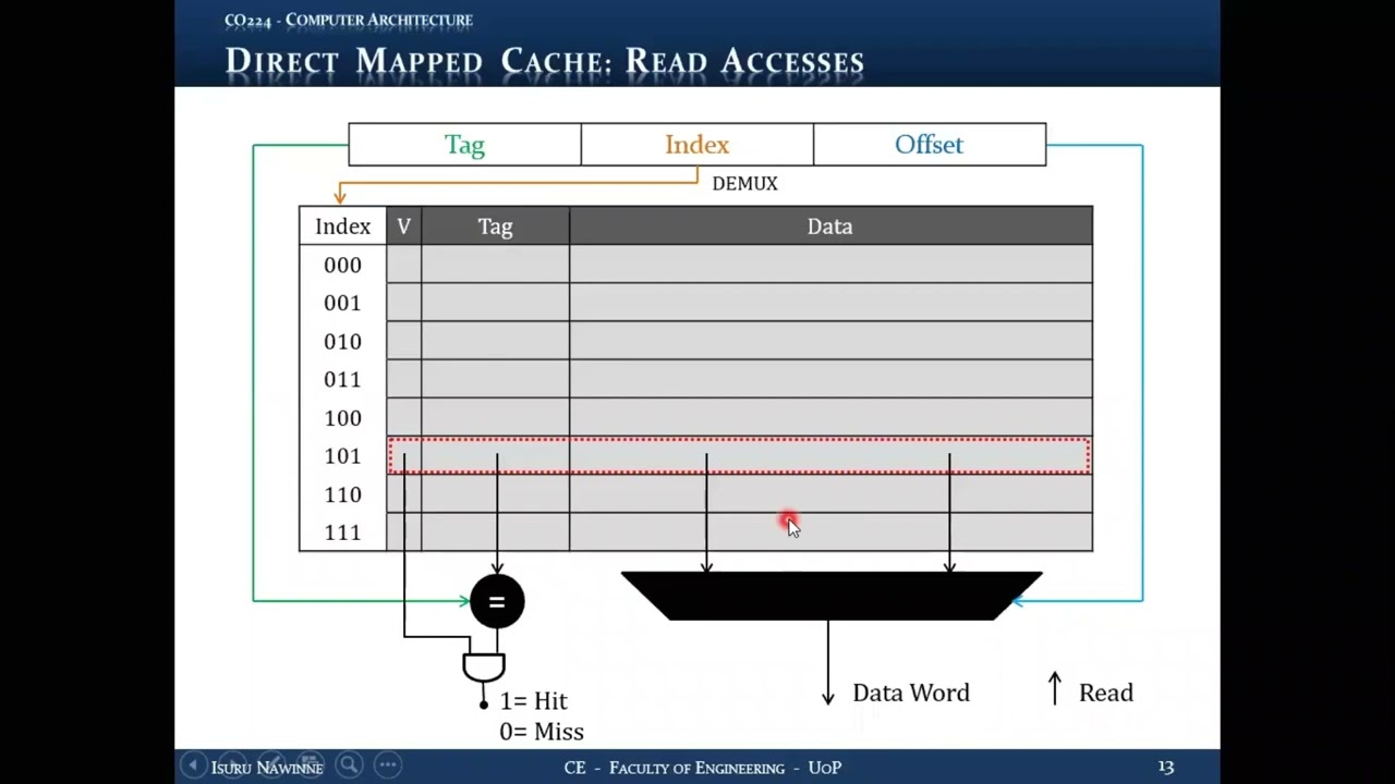
Step 1: Address Decomposition
- Parse incoming address into three fields:
- Tag: For verification
- Index: For cache entry selection
- Offset: For word/byte selection within block
Step 2: Cache Entry Selection (Indexing)
- Extract index bits from address
- Cache controller knows which bits are index (by design)
- Use demultiplexer circuitry to access correct cache entry
- Example: Index = 101 (binary) → Access cache entry 5
- Direct access, no search needed
- Combinational logic (fast)
Step 3: Tag Comparison
- Extract stored tag from selected cache entry
- Extract tag from incoming address
- Use comparator circuit (XNOR gates + AND gate)
- Output: 1 if tags match, 0 if tags differ
Step 4: Valid Bit Check
- Extract valid bit from selected cache entry
- Check if entry contains valid data
- Output: 1 if valid, 0 if invalid
Step 5: Hit/Miss Determination
- Logic: Hit = (Tag Match) AND (Valid Bit)
- If both conditions true → HIT
- If either condition false → MISS
- Single AND gate combines both signals
Step 6: Data Extraction (Parallel Operation)
- Happens simultaneously with tag comparison
- Extract entire data block from cache entry
- Place data block on internal wires
- Example: 8-byte block = 2 words
Step 7: Word Selection (Using Offset)
- CPU requests a single WORD
- Use word offset bits as MUX select signal
- Example: 2 words in block
- Offset MSB = 0 → Select first word
- Offset MSB = 1 → Select second word
- Multiplexer extracts correct word from block
15.3.3 Timing Optimization
Parallel Operations:
- Tag comparison (Steps 3-5) and data extraction (Steps 6-7) happen in PARALLEL
- Both are combinational circuits
- Total delay = max(tag comparison delay, data extraction delay)
- Reduces overall hit latency
15.3.4 Read Hit Outcome
- Selected word is correct data
- Send word to CPU immediately
- No stall required
- Total time: Hit latency (< 1 nanosecond for SRAM)
- Completes within one CPU clock cycle
- Pipeline continues uninterrupted
15.3.5 Pipeline Integration
- In MIPS pipeline, MEM stage accesses memory
- With cache hit: Memory access completes in 1 cycle
- Pipeline maintains smooth operation
- No bubbles inserted
15.4 Cache Read Miss Handling
15.4.1 Read Miss Scenario
Miss Conditions
- Tag mismatch (most common)
- Requested block not in cache
- Different block occupies that cache location
- Invalid entry
- Valid bit = 0
- Entry contains no valid data (e.g., after initialization)
- Both conditions
- Tag mismatch AND invalid entry
15.4.2 Read Miss Response Required Actions
Action 1: STALL THE CPU
Process:
- CPU cannot proceed without requested data
- Data hazard would occur if CPU continues
- Cache controller sends STALL signal to CPU
- CPU must monitor stall signal continuously
- When stall signal high → Freeze CPU operation
- Stop fetching new instructions
- Freeze all pipeline stages
- Hold current state
CPU's Perspective:
- CPU doesn't know cache and memory are separate
- CPU sees memory hierarchy as single "memory"
- Must respond to stall signal from memory subsystem
- In MEM stage: Check and respond to stall signal
Action 2: MAKE READ REQUEST TO MAIN MEMORY
Request Details:
- Request the missing DATA BLOCK (not just word!)
- Cache and memory trade in BLOCKS
- CPU trades in words/bytes, but cache-memory interface uses blocks
- Send block address to main memory
- Memory fetches entire block
Reason for Block Transfer:
- Exploits spatial locality
- Fetches requested word AND nearby words
- Reduces future misses for nearby addresses
- More efficient than fetching single words
Memory Access Time:
- DRAM access: Several CPU clock cycles
- Range: 10 to 100+ CPU clock cycles
- Much slower than cache (< 1 cycle)
- This is the MISS PENALTY
Action 3: WAIT FOR MEMORY RESPONSE
- Memory performs read operation
- Data travels from memory to cache
- Controller waits (CPU still stalled)
- Multiple clock cycles elapse
Action 4: UPDATE CACHE ENTRY
Three components to update:
a) Update Data Block:
- Write fetched block into cache entry
- Replace old data at that index
b) Update Tag:
- Extract tag from block address
- Write tag into tag array at that index
- Ensures future tag comparisons work correctly
c) Set Valid Bit:
- Set valid bit to 1
- Denotes entry now contains valid data
Action 5: SEND DATA TO CPU
- Extract requested word from newly loaded block
- Use offset to select correct word
- Put data on bus to CPU
- CPU receives requested data
Action 6: CLEAR STALL SIGNAL
- Cache controller clears (lowers) stall signal
- CPU detects stall signal going low
- CPU resumes operation
- Pipeline unfreezes and continues
15.4.3 Total Read Miss Time
Formula:
Read Miss Time = Hit Latency + Miss Penalty
Where:
- Hit Latency: Time to determine it's a miss (< 1 ns)
- Miss Penalty: Time to fetch from memory (10-100+ CPU cycles)
Example Calculation:
- Hit latency: 1 ns (1 cycle at 1 GHz)
- Miss penalty: 50 ns (50 cycles at 1 GHz)
- Total: 1 + 50 = 51 cycles
15.4.4 Performance Impact
- Single miss causes 50+ cycle stall
- Catastrophic for pipeline performance
- Emphasizes need for high hit rate (> 99.9%)
15.4.5 Question: What About the Old Block?
The Deferred Question:
- When fetching new block on miss
- Old block occupies that cache entry
- What happens to old block?
- Is it okay to discard it?
- Answer depends on write policy
- Need to understand writes first
- Question will be revisited
15.5 Cache Write Access - Introduction
15.5.1 Write Access Input Signals
From CPU to Cache Controller:
- Address (where to write)
- Data Word (what to write)
- Write Control Signal (indicates write operation)
Three inputs vs. two for read (no data input needed for read).
15.5.2 Write Access Process
Step 1: Address Decomposition
- Same as read: [Tag][Index][Offset]
Step 2: Cache Entry Selection
- Same as read: Use index bits
- Demultiplexer accesses correct entry
- Direct access based on index
- Example: Index 101 → Entry 5
Step 3: Tag Comparison
- Extract tag from cache entry
- Compare with incoming address tag
- Comparator circuit (same as read)
- Output: Match or no match
Step 4: Valid Bit Check
- Extract and check valid bit
- Same as read operation
- Ensures entry is valid
Step 5: Hit/Miss Determination
- Hit = (Tag Match) AND (Valid Bit)
- Same logic as read
- Determines write hit or write miss
Step 6: Data Writing (The Difference)
This is where write differs from read:
- Must write data word to correct location in block
- Use offset to determine which word in block
15.5.3 Writing Mechanism
Input:
- Incoming data word (from CPU)
- Offset bits from address
Demultiplexer Selection:
- Use word offset as demultiplexer select signal
- Example with 2 words per block:
- Word offset = 0 → Write to first word
- Word offset = 1 → Write to second word
- Demultiplexer directs data to correct word position
Example:
- Block has 2 words: Word0 (bytes 0-3), Word1 (bytes 4-7)
- Incoming data word: 0x12345678
- Offset MSB = 1 → Select Word1
- Demux directs data to Word1 position in block
Write Operation Control:
- Writing controlled by Write control signal from CPU
- Only write if signal indicates write operation
- Demultiplexer enabled by write signal
15.5.4 Critical Question: Can Write and Tag Compare Happen in Parallel?
For Read (Previous Discussion)
- YES, both can happen in parallel
- If miss, discard extracted data (no harm done)
- Reading doesn't change cache state
For Write (Current Question)
More problematic!
- What if we write and then discover tag mismatch?
Scenario:
- Write to cache entry simultaneously with tag comparison
- Tag comparison returns MISMATCH
- We've now CORRUPTED data in cache!
- Written to wrong block (different tag)
- Data integrity violated
Problem:
- If invalid entry: Not too serious (data was garbage anyway)
- If tag mismatch: SERIOUS problem!
- Overwrote valid data for different block
- That block's data now corrupted
- Future accesses to that block get wrong data
Initial Conclusion:
- Cannot safely write and tag compare in parallel
- Need mechanism to prevent corruption
- Solution depends on write policy (discussed next)
15.6 Write Policies - Introduction
15.6.1 The Data Consistency Problem
Scenario:
- CPU writes to address A
- Address A hits in cache
- Cache controller writes new value to cache entry
- Cache now has updated value
- Main memory still has OLD value
- Two versions exist: Cache version ≠ Memory version
The Inconsistency:
- Cache entry now INCONSISTENT with main memory
- Same address has different values in different levels
- Data coherence problem
15.6.2 Why This Matters
- Future access to same address: Which value is correct?
- If cache entry replaced: New value lost
- I/O devices may access memory directly (bypass cache)
- Multi-processor systems: Other CPUs access memory
- Must maintain data consistency across hierarchy
15.6.3 Two Fundamental Write Policies
- Write-Through (discussed this lecture)
- Write-Back (mentioned, detailed in next lecture)
15.7 Write-Through Policy
15.7.1 Write-Through Definition
Policy Statement:
> "Always write to BOTH cache AND memory"
Mechanism:
- On every write operation:
- Write to cache (if hit)
- Simultaneously write to main memory
- Both levels updated together
- Ensures cache and memory always consistent
15.7.2 Write-Through Process
Write Hit with Write-Through
- Determine it's a write hit (tag match + valid)
- Write data word to cache block (using offset)
- Also send write request to main memory
- Update same address in memory
- Wait for memory write to complete
- Both cache and memory now have same value
Write Miss with Write-Through
- Determine it's a write miss
- Stall CPU
- Fetch missing block from memory (read operation)
- Update cache entry with fetched block
- Write the word to correct position in block
- Also write to memory
- Clear stall signal
- Both levels updated
15.7.3 Advantages of Write-Through
Advantage 1: SIMPLICITY
- Straightforward to implement
- No complex consistency protocols
- Cache controller logic simpler
- Design principle: Keep cache simple
Advantage 2: CONSISTENCY GUARANTEED
- Cache and memory ALWAYS have same values
- No special handling for discarded blocks
- Can replace any cache entry anytime
- Memory always has correct, up-to-date data
Advantage 3: ANSWERS THE OLD BLOCK QUESTION
With write-through policy:
- Old block can be safely discarded
- All updates were written to memory
- Memory has latest version
- Future accesses can fetch from memory
- No data loss
Comparison:
- Read miss: Old block discarded, data available in memory
- Write with write-through: Always updated memory, safe to discard
Advantage 4: PARALLEL WRITE AND TAG COMPARE NOW POSSIBLE!
Critical Insight:
Can now overlap write and tag comparison. Why? Two scenarios:
Scenario A: Write Hit
- Written to cache, will also write to memory
- Tag matches, write is correct
- Both cache and memory updated
- No problem
Scenario B: Write Miss
- Written to cache entry (possibly wrong block)
- Tag mismatch detected
- Will fetch correct block from memory anyway
- Will overwrite cache entry with correct block
- Corrupted data gets replaced immediately
- Memory has correct version (wasn't corrupted)
- No lasting damage
Result:
- Safe to write and tag compare in parallel
- Saves time (hit latency reduced)
- Both operations in same clock cycle
- If hit: Saved time
- If miss: No harm (will fix cache anyway)
Timing Optimization:
Tag comparison time: T_comp
Write time: T_write
Without overlap: Total = T_comp + T_write
With overlap: Total = max(T_comp, T_write)
Typically similar delays → Nearly 2× speedup
15.7.4 Disadvantages of Write-Through
Disadvantage 1: EXCESSIVE WRITE TRAFFIC
- EVERY write goes to memory
- Memory writes are slow (10-100+ cycles)
- Generates continuous memory traffic
- Memory bus congestion
Disadvantage 2: CPU STALLS ON EVERY WRITE
Critical Problem:
- Every write requires memory access
- Memory much slower than cache
- CPU must stall for EVERY write
- Wait for memory write to complete
Stall Duration:
- Memory write: 10-100 CPU clock cycles
- Every store instruction causes stall
- Even on write HIT!
Example:
- Store instruction hits in cache
- Still must wait for memory write
- 50 cycle stall for every store
- Pipeline essentially stops
Impact on Programs with Many Writes:
- Programs with frequent store instructions
- Array updates, structure modifications
- Loop counters being updated
- String manipulation
- All suffer severe performance degradation
Performance Comparison:
- Read hit: < 1 cycle (fast!)
- Write hit with write-through: 50+ cycles (slow!)
- Asymmetry: Reads fast, writes catastrophically slow
Pipeline Impact:
- Recall pipelining lectures: Minimized stalls
- Worked hard to avoid 1-2 cycle stalls
- Write-through introduces 50+ cycle stalls regularly
- Contradicts pipeline optimization goals
- "Doesn't add up" - unacceptable performance loss
Real-World Issue:
- Write-through used in some systems
- But with additional optimizations (write buffers, discussed later)
- Pure write-through too slow for modern systems
Disadvantage 3: POWER CONSUMPTION
- Memory accesses consume power
- Every write → Memory access → Power consumption
- Unnecessary power usage
- Critical for mobile/embedded systems
Disadvantage 4: MEMORY WEAR
- Flash memory: Limited write cycles
- SSDs wear out with writes
- Write-through accelerates wear
- Reduces memory lifespan
15.8 Resolving the Old Block Question
15.8.1 The Question Revisited
Original Question:
> "What happens to the old block when we fetch a new block from memory on a miss?"
Context:
- Read or write miss occurs
- Need to fetch missing block from memory
- Old block occupies target cache entry
- Must replace old block with new block
- Is it safe to discard old block?
15.8.2 Answer with Write-Through Policy
YES, Safe to Discard
Reason 1: Memory Has Updated Version
- Write-through ensures every write goes to memory
- All modifications reflected in memory
- Memory always has latest version of all blocks
- Old block's latest state is in memory
Reason 2: Can Re-fetch If Needed
- Future access to old block's address
- Will miss in cache (block was replaced)
- Can fetch from memory again
- Memory has correct, up-to-date data
- No data loss
15.8.3 Example Scenario
- Block A in cache at index 3
- Block A modified several times
- Each modification written to cache AND memory
- Block B (also maps to index 3) is requested
- Miss occurs for Block B
- Fetch Block B from memory
- Replace Block A with Block B at index 3
- Block A discarded from cache
- Block A's data safe in memory
- Later access to Block A: Miss, fetch from memory again
15.8.4 Comparison with Invalid Entry
- If miss due to invalid bit: Obviously safe to replace
- If miss due to tag mismatch: Safe because of write-through
15.8.5 Contrast with Future Policy (Teaser)
- With other write policies (write-back), answer may differ
- May NOT be safe to discard old block
- Will discuss in next lecture
Conclusion:
- Write-through simplifies replacement
- No special checks needed before replacing block
- Always safe to overwrite cache entry
- Memory serves as reliable backup
15.9 Parallelism in Write Access with Write-Through
15.9.1 The Parallel Write Problem Solved
Original Concern:
- Want to overlap write operation and tag comparison
- Reduce hit latency
- But risk corrupting data if tag mismatch
15.9.2 With Write-Through Policy
Case 1: Write Hit
- Write to cache and tag compare happen in parallel
- Tag matches → It was a hit
- Cache entry correctly updated
- Also write to memory (per write-through policy)
- Both cache and memory consistent
- Time saved: One cycle
- No problem!
Case 2: Write Miss
- Write to cache and tag compare happen in parallel
- Tag doesn't match → It was a miss
- Cache entry might be corrupted (wrote to wrong block)
- BUT: About to fetch correct block from memory
- Will OVERWRITE this cache entry with new block
- Corrupted data disappears immediately
- Also, write goes to memory (correct address in memory)
- End result: Cache fixed, memory correct
15.9.3 Key Insight
- Write-through to memory preserves correctness
- Memory write goes to CORRECT address (from address bus)
- Even if cache entry temporarily corrupted
- Cache entry will be fixed when correct block loaded
- Memory never corrupted
15.9.4 Timeline for Write Miss
Cycle 1: Write to cache (possibly wrong block) + Tag compare
Cycle 1: Also initiate memory write (correct address)
Cycle 2-50: Fetch correct block from memory
Cycle 51: Overwrite cache entry with correct block
Result: Cache correct, memory correct
15.9.5 Safety Guarantee
- Memory write: Targets address from address bus (always correct)
- Cache write: Targets index (might be for different block)
- If miss: Cache mistake corrected by fetch
- If hit: No mistake, everything correct
- In both cases: End state correct
15.9.6 Performance Benefit
- Saved cycles on write hit path
- Write and tag compare: Parallel instead of sequential
- Approximately 2× faster hit determination
- Critical for frequent write hits
15.9.7 Enabled by Write-Through
- Only possible because memory updated on every write
- Other policies may not allow this optimization
- Write-through sacrifices write performance for simplicity
- But enables some optimizations
15.10 Summary of Cache Operations
15.10.1 Complete Cache Operation Overview
READ HIT
- Index → Tag compare + Valid check → Match
- Extract data block → Select word → Send to CPU
- Time: < 1 cycle (hit latency only)
- No stall
- Pipeline continues
READ MISS
- Index → Tag compare + Valid check → No match
- Stall CPU
- Fetch block from memory (10-100+ cycles)
- Update cache: Data + Tag + Valid bit
- Extract word → Send to CPU
- Clear stall
- Time: Hit latency + Miss penalty
- Major pipeline disruption
WRITE HIT (with Write-Through)
- Index → Tag compare + Valid check (parallel with write)
- Write word to cache block
- Also write to memory (10-100+ cycles)
- Stall CPU until memory write completes
- Time: Hit latency + Memory write time
- Slower than read hit!
WRITE MISS (with Write-Through)
- Index → Tag compare + Valid check → No match
- Stall CPU
- Fetch block from memory
- Update cache: Data + Tag + Valid bit
- Write word to cache block
- Also write to memory
- Clear stall
- Time: Hit latency + Miss penalty + Memory write time
- Even slower than read miss!
15.10.2 Performance Characteristics
| Case | Time | Comment |
|---|---|---|
| Best Case (Read Hit) | < 1 cycle | Optimal performance. Want this to be most common case |
| Moderate Case (Read Miss) | 50+ cycles | Acceptable if infrequent. Reason for high hit rate requirement |
| Poor Case (Write Hit with Write-Through) | 50+ cycles | Every write hits this case. Unacceptable for write-heavy programs |
| Worst Case (Write Miss with Write-Through) | 100+ cycles | Rare but extremely slow. Catastrophic when occurs |
Performance Goal:
- Maximize read hits
- Minimize write impact (better policy needed)
- Overall hit rate > 99.9%
15.11 Write-Through Policy Evaluation
15.11.1 Summary of Write-Through
Mechanism:
- Write to cache (if hit) AND memory
- Always keep both consistent
- Memory is authoritative backup
Implementation Complexity:
- Simple cache controller logic
- No complex state tracking
- Straightforward consistency maintenance
15.11.2 Advantages
| Advantage | Description |
|---|---|
| 1. Simplicity | Easy to understand, simple to implement, minimal controller complexity, aligns with design principle (simple cache) |
| 2. Consistency | Cache and memory always consistent, no special synchronization needed, can discard blocks anytime, memory always reliable |
| 3. Data Safety | No data loss on block replacement, memory has all updates, crash recovery simpler, I/O devices see correct data |
| 4. Enables Optimizations | Can overlap write and tag compare, reduces hit latency, safe due to memory backup |
15.11.3 Disadvantages
| Disadvantage | Description |
|---|---|
| 1. Performance Penalty | Every write stalls CPU, 10-100+ cycle stalls per write, unacceptable for write-intensive programs, contradicts pipeline optimization goals |
| 2. Memory Traffic | Excessive write traffic to memory, memory bus congestion, reduces available bandwidth for read misses, slows down entire system |
| 3. Power Consumption | Every write powers up memory, unnecessary power usage, battery drain in mobile devices, heat generation |
| 4. Memory Wear | Flash/SSD: Limited write cycles, accelerated wear-out, reduced memory lifespan, particularly bad for SSDs |
15.11.4 When Write-Through Used
Suitable Applications
- Read-heavy workloads
- Simple embedded systems
- Systems requiring guaranteed consistency
- Safety-critical applications
Real-World Usage
- Often combined with write buffers
- Write buffer: Small queue for pending writes
- CPU continues after writing to buffer
- Buffer drains to memory in background
- Reduces stall impact (will discuss if time permits)
Modern Systems
- Pure write-through rarely used alone
- Too slow for general-purpose computing
- Alternative: Write-back policy (next lecture)
- Trade complexity for performance
15.12 The Need for Alternative Write Policies
15.12.1 The Performance Problem
Write-Heavy Programs
Many programming patterns involve frequent writes:
- Array updates in loops
- Data structure modifications
- Counter increments
- Accumulator updates
- String/buffer operations
Example Code:
for (int i = 0; i < 1000; i++) {
    array[i] = compute(i);  // Store in every iteration
    sum += array[i];         // Read, accumulate, store
}
With Write-Through
- Loop iterations: 1000
- Stores per iteration: 2 (array[i], sum)
- Total stores: 2000
- Cycles per store: 50 (memory write)
- Total stall cycles: 100,000!
- Versus computation cycles: Maybe 10,000
- Performance: 10× slower than necessary!
15.12.2 Pipeline Impact
- Pipelining designed to execute 1 instruction/cycle (ideal)
- Write-through: 50 cycles per store instruction
- Pipeline utilization: ~2% (1/50)
- Completely defeats pipelining benefits
15.12.3 Comparison with Read Operations
| Operation | Time | Frequency | Acceptability |
|---|---|---|---|
| Read hit | < 1 cycle | Common | Fast |
| Read miss | 50 cycles | Rare | Acceptable |
| Write hit | 50 cycles | Frequent | Unacceptable |
| Write miss | 100+ cycles | Rare | Terrible |
15.12.4 The Contradiction
- Spent lectures optimizing pipeline
- Minimized hazards, used forwarding, prediction
- Eliminated 1-2 cycle stalls
- Now introducing 50+ cycle stalls on every write!
- "Doesn't add up" - need better solution
15.12.5 Question Raised
"What can we do to avoid this situation?"
Student Insight:
"We can write to memory only when we want to replace that cache block with different data"
Instructor Response:
"Exactly! That becomes a different write policy."
15.12.6 Teaser for Next Lecture
- Alternative policy: Write-Back
- Write to cache only, not memory immediately
- Write to memory only when necessary
- Much better performance
- Added complexity in return
- Will discuss in detail next class
15.13 Lecture Conclusion
15.13.1 Topics Covered
1. Complete Read Access Process
- Index → Tag compare → Valid check → Hit/Miss
- Parallel data extraction and word selection
- Hit: Send data immediately
- Miss: Fetch from memory, stall CPU
2. Read Miss Handling
Six-step process:
- Stall CPU
- Request block from memory
- Wait for response
- Update cache entry (data, tag, valid)
- Send data to CPU
- Clear stall
- Miss penalty: 10-100+ cycles
3. Write Access Process
- Similar to read: Index → Tag compare → Valid check
- Difference: Must write data to cache
- Use demultiplexer to direct data to correct word
4. Data Consistency Problem
- Writing to cache creates inconsistency
- Cache has new value, memory has old value
- Need policy to maintain consistency
5. Write-Through Policy
- Write to both cache and memory on every write
- Advantages: Simple, consistent, safe
- Disadvantages: Slow, excessive traffic, poor performance
6. Old Block Question Resolved
- With write-through: Safe to discard
- Memory has updated version
- Can re-fetch if needed later
7. Parallel Write Optimization
- Can overlap write and tag compare
- Write-through makes this safe
- Reduces hit latency
8. Performance Issues
- Write-through too slow for write-intensive programs
- Every write causes long stall
- Need better policy
15.13.2 Next Lecture Preview
Topics to Cover:
- Write-Back policy (delayed writes)
- Dirty bit concept
- When to write back to memory
- Performance improvements
- Complexity tradeoffs
- Block replacement with write-back
- Comparison: Write-through vs. Write-back
- Real-world cache designs
Implementation Details:
- Write buffer optimization for write-through
- Handling dirty blocks on replacement
- Write-back state machine
- Performance analysis
Advanced Topics (if time):
- Write-allocate vs. no-write-allocate
- Write-combining
- Victim caches
- Multi-level caches with different policies
The Goal:
- Understand tradeoffs between simplicity and performance
- Choose appropriate policy for application
- Design efficient cache systems
Key Insight:
Write-through sacrifices performance for simplicity. In modern systems, performance is critical, so more complex policies are necessary despite added complexity.
Key Takeaways
- Cache read hit completes in single cycle—tag match and valid bit set indicate data available immediately from cache.
- Cache read miss requires multiple cycles—must fetch entire block from main memory, update cache entry, set valid bit, then retry access.
- Cache controller implements state machine—managing transitions between idle, compare tags, fetch block, and write cache states.
- Tag comparison determines hit/miss—stored tag must match address tag AND valid bit must be set for successful hit.
- Block fetch retrieves entire block from memory—exploiting spatial locality by bringing multiple words that will likely be accessed soon.
- Valid bit initialization crucial at startup—all valid bits cleared to zero, preventing false hits on random cache data.
- Write operations complicate cache design—must maintain consistency between cache and main memory through careful policy choices.
- Write-through policy updates both cache and memory on every write—simple consistency but severe performance penalty.
- Write-through advantages: Simple implementation, main memory always current, no dirty bit needed, straightforward crash recovery.
- Write-through disadvantages: Every write causes slow memory access (~100 ns), dramatically reduces performance, wastes memory bandwidth.
- Write buffers partially mitigate write-through penalty—CPU writes to buffer and continues, buffer writes to memory asynchronously.
- Write buffer depth typically 4-8 entries—balances performance improvement against hardware cost and complexity.
- Write buffer full forces CPU stall—occurs during write-intensive code sections, limiting write-through effectiveness.
- Write miss policies determine cache behavior—write-allocate (fetch block first) versus no-write-allocate (write directly to memory).
- Write-allocate exploits temporal locality—if just written location likely accessed again soon, fetching to cache improves future performance.
- No-write-allocate avoids fetch overhead—appropriate when written locations unlikely to be accessed soon.
- Policy combinations affect overall performance—write-through typically paired with no-write-allocate for consistency.
- Cache consistency means cache and memory agree on data values—critical correctness requirement across all cache operations.
- Performance impact of write policies substantial—write-through can increase memory traffic by 15-20% in typical programs.
- Write-back policy introduced as superior alternative—defers memory writes until block eviction, dramatically reducing memory traffic.
Summary
Detailed examination of cache memory operations reveals the sophisticated control logic required to manage read and write accesses while maintaining data consistency between cache and main memory. Read operations follow straightforward paths: hits deliver data in single cycle via tag comparison confirming both tag match and valid bit set, while misses trigger multi-cycle sequences fetching entire blocks from main memory, updating cache entries, setting valid bits, and retrying accesses. The cache controller implements these sequences through state machine logic managing transitions between idle, tag comparison, block fetching, and cache writing states. Write operations introduce significant complexity and performance implications through policy choices determining how cache and memory stay synchronized. Write-through policy, updating both cache and memory on every write, offers simplicity and guaranteed consistency—main memory always reflects current data state, enabling straightforward crash recovery and multi-processor coherence. However, write-through's performance penalty proves severe: every write operation incurs ~100 nanosecond memory access delay, effectively eliminating cache benefit for write-heavy code sections and wasting substantial memory bandwidth on updates. Write buffers provide partial mitigation by decoupling CPU from memory write delays, allowing processors to write to small hardware queues and continue execution while buffer contents asynchronously propagate to main memory. Typical write buffers holding 4-8 entries balance performance improvement against hardware cost, though write-intensive code can still fill buffers and force CPU stalls. Write miss policies—write-allocate (fetch block before writing) versus no-write-allocate (write directly to memory)—represent additional design choices affecting performance based on program access patterns. Write-allocate exploits temporal locality, benefiting code that writes then soon reads same locations, while no-write-allocate avoids fetch overhead for write-once scenarios. Write-through typically pairs with no-write-allocate for policy consistency. The fundamental limitation—that write-through forces memory access on every write regardless of whether data will be accessed again—motivates write-back policies introduced in subsequent lectures, which defer memory writes until block eviction and thereby dramatically reduce memory traffic. Understanding these operational details and policy tradeoffs proves essential for appreciating how real cache implementations balance performance, complexity, consistency, and correctness requirements in practical computer systems.