Control Unit Design
Control Signals Generated from the OPCODE
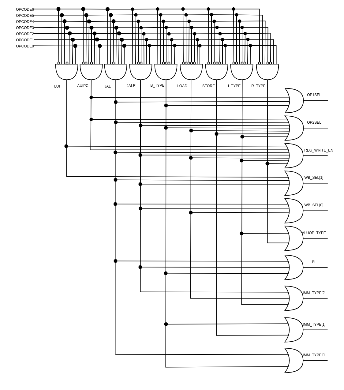
Control unit was implemented using combinational logic. Some control signals were generated by using the OPCODE bits in the instruction and for some control signals an intermediate signal was generated using the OPCODE bits and then the intermediate signal, FUNCT3 bits and FUNCT7 bits of the instruction were used to generate the control signals.
Control signals generated using the OPCODE,
- OP1_SEL
- OP2_SEL
- MEM_WRITE
- MEM_READ
- REG_WRITE_EN
- WB_SEL[1:0]
Control signals generated using the OPCODE, FUNCT3 and FUNCT7,
- IMM_SEL[2:0]
- ALU_OP[4:0]
- BRANCH_JUMP[2:0]
Figure 3 shows the combinational logic circuit designed to generate the control signals and the intermediate signals using the OPCODE bits. ALUOP_TYPE, BL and IMM_TYPE are the intermediate signals generated using the OPCODE bits which will be later used by separate combinational logic circuits to generate the ALU_OP, BRANCH_JUMP and IMM_SEL control signals respectively.
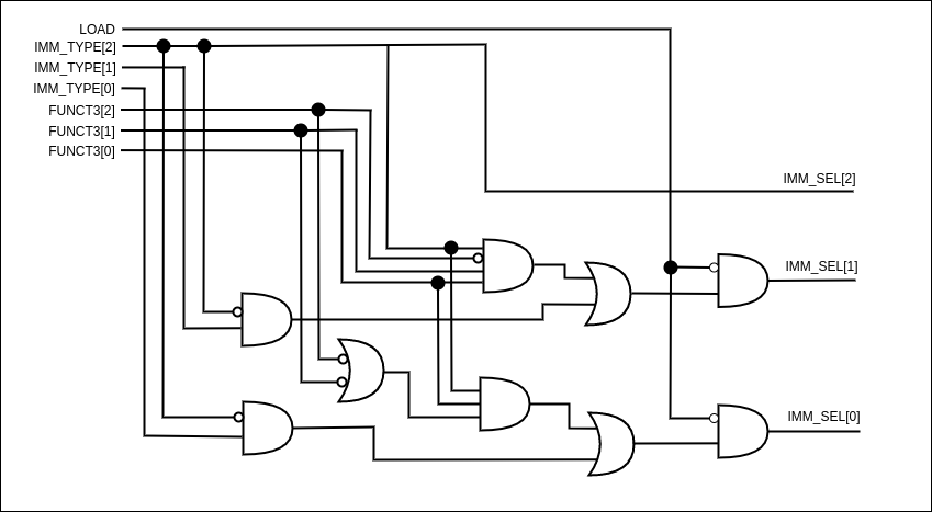
Generating the IMM_SEL control signal
To generate the IMM_SEL control signal, the FUCNT3 bits of the instruction were used to obtain the proper immediate variant for the instructions given below.
- SLTIU - This is the only instruction that requires an unsigned immediate variant.
- SLLI, SRLI, SRAI - These instructions require the immediate variant that contains the shift amount.
FUNCT3 bits in SLTIU, SLLI, SRLI and SRAI instructions were used along with the IMM_TYPE intermediate signal to generate the IMM_SEL control signal.
| Immediate Type | IMM_TYPE[2] | IMM_TYPE[1] | IMM_TYPE[0] | FUNCT3[2] | FUNCT3[1] | FUNCT3[0] | IMM_SEL[2] | IMM_SEL[1] | IMM_SEL[0] |
|---|---|---|---|---|---|---|---|---|---|
| - | Inputs | Inputs | Inputs | Inputs | Inputs | Inputs | Outputs | Outputs | Outputs |
| U | 0 | 0 | 0 | x | x | x | 0 | 0 | 0 |
| J | 0 | 0 | 1 | x | x | x | 0 | 0 | 1 |
| S | 0 | 1 | 0 | x | x | x | 0 | 1 | 0 |
| B | 0 | 1 | 1 | x | x | x | 0 | 1 | 1 |
| I_signed | 1 | 0 | 0 | x | x | x | 1 | 0 | 0 |
| I_shift | 1 | 0 | 0 | x | 0 | 1 | 1 | 0 | 1 |
| I_unigned | 1 | 0 | 0 | 0 | 1 | 1 | 1 | 1 | 1 |
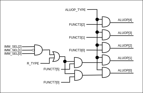
Generating the ALU_OP control signal
ALUOP_TYPE intermediate signal, FUNCT3, FUNCT7, IMM_SEL control signal, and R_TYPE(generated from the OPCODE) were used to generate the ALU_OP control signal. 4 variants can be considered when generating the control signal.
-
R - Type, SLLI, SRLI and SRAI instructions ALU_OP for these instructions were generated by concatenating the 3 bits in the FUNCT3, 5th bit in FUNCT7 and 0th bit in the FUNCT7.
-
I - Type instructions without SLLI, SRLI and SRAI instructions ALU_OP for these instructions were generated by concatenating the 3 bits in the FUNCT3, 2 zero signals.
-
All other instructions that uses ALU ALU_OP for these instructions was an ADD operation.
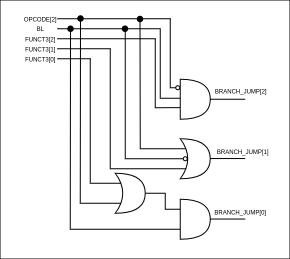
Generating the BRANCH_JUMP control signal
BL intermediate signal, OPCODE[2] and FUNCT3 bits were used to generate the BRANCH_JUMP control signal. In B - Type instructions, the FUNCT3 bits define the type of branching. Therefore FUNCT3 bits were used to identify the branch type. OPCODE[2] bit was used to distinguish between the B - Type and the J - Type instructions.
| Branch Type | OPCODE[2] | BL | FUNCT3[2] | FUNCT3[1] | FUNCT3[0] | BRANCH_JUMP[2] | BRANCH_JUMP[1] | BRANCH_JUMP[0] |
|---|---|---|---|---|---|---|---|---|
| - | Inputs | Inputs | Inputs | Inputs | Inputs | Outputs | Outputs | Outputs |
| BEQ | 0 | 1 | 0 | 0 | 0 | 0 | 0 | 0 |
| BNE | 0 | 1 | 0 | 0 | 1 | 0 | 0 | 1 |
| NO | x | 0 | x | x | x | 0 | 1 | 0 |
| J | 1 | 1 | x | x | x | 0 | 1 | 1 |
| BLT | 0 | 1 | 1 | 0 | 0 | 1 | 0 | 0 |
| BGE | 0 | 1 | 1 | 0 | 1 | 1 | 0 | 1 |
| BLTU | 0 | 1 | 1 | 1 | 0 | 1 | 1 | 0 |
| BGEU | 0 | 1 | 1 | 1 | 1 | 1 | 1 | 1 |
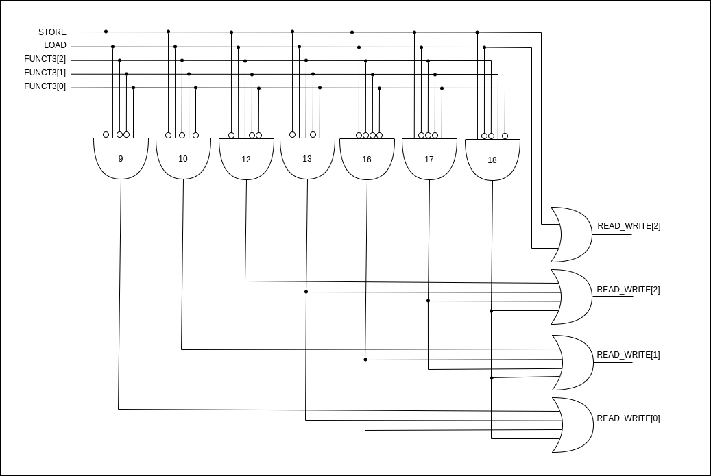
Generating the READ_WRITE control signal
FUNCT3 bits, LOAD and STORE (LOAD and STORE by decoding the OPCODE) signals were used to generate the READ_WRITE control signal. LOAD and STORE signals are asserted when the instruction is a LOAD or a STORE instruction respectively. FUNCT3 bits were used to determine the number of bits (8 bit, 16 bit, 32 bit) loaded/stored.
When the instruction is a LOAD or a STORE, the READ_WRITE[3] bit will get asserted and by using only the READ_WRITE[3] bit, the data cache memory can assert the BUSYWAIT signal and the remaining bits of the READ_WRITE signal will determine the number of bits stored.. If the instruction is not a LOAD or a STORE the READ_WRITE[3] bit is cleared.
| Load/Store Type | STORE | LOAD | FUCNT3[2] | FUCNT3[1] | FUCNT3[0] | READ_WRITE[3] | READ_WRITE[2] | READ_WRITE[1] | READ_WRITE[0] |
|---|---|---|---|---|---|---|---|---|---|
| No load/store | 0 | 0 | x | x | x | 0 | 0 | 0 | 0 |
| No load/store | 1 | 1 | x | x | x | 0 | 0 | 0 | 0 |
| LB | 0 | 1 | 0 | 0 | 0 | 1 | 0 | 0 | 0 |
| LH | 0 | 1 | 0 | 0 | 1 | 1 | 0 | 0 | 1 |
| LW | 0 | 1 | 0 | 1 | 0 | 1 | 0 | 1 | 0 |
| LBU | 0 | 1 | 1 | 0 | 0 | 1 | 1 | 0 | 0 |
| LHU | 0 | 1 | 1 | 0 | 1 | 1 | 1 | 0 | 1 |
| SB | 1 | 0 | 0 | 0 | 0 | 1 | 0 | 1 | 1 |
| SH | 1 | 0 | 0 | 0 | 1 | 1 | 1 | 1 | 0 |
| SW | 1 | 0 | 0 | 1 | 0 | 1 | 1 | 1 | 1 |