Data Cache
Data cache sits in between the CPU and the data memory. When the CPU loads/stores data from/to the data cache, depending on the validity of the data blocks stored in the cache it will undergo a hit or a miss.
In the case of a hit, the cache will read/write the data from/to the cache. This will not stall the CPU.
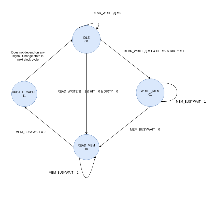
In the case of a miss, the cache will stall the CPU and fetch the correct block from the memory and update the cache.Once the cache is updated, the CPU can read/write the data from/to the cache.
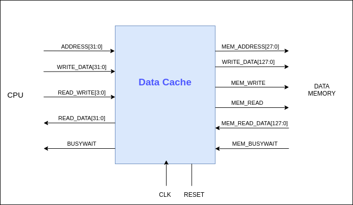
Inputs to Data Cache from CPU are,
- ADDRESS[31:0]
- WRITE_DATA[31:0]
- READ_WRITE[3:0]
Outputs from Data Cache to CPU are,
- READ_DATA[31:0]
- BUSYWAIT
Inputs to Data Cache from Data Memory are,
- MEM_READ_DATA[127:0]
- MEM_BUSYWAIT
Outputs from Data Cache to Data Memory are,
- MEM_ADDRESS[27:0]
- WRITE_DATA[127:0]
- MEM_WRITE
- MEM_READ
When the CPU sends an address to the cache and if the READ_WRITE[3] bit of the control signal is set, the cache will set the BUSYWAIT signal to stall the CPU. Then the cache will check if the address is a hit or a miss. Once the operations in the cache are completed and the CPU is served, the cache has to clear the BUSYWAIT.Clearing of the BUSYWAIT signal will happen at the next positive edge of the clock.
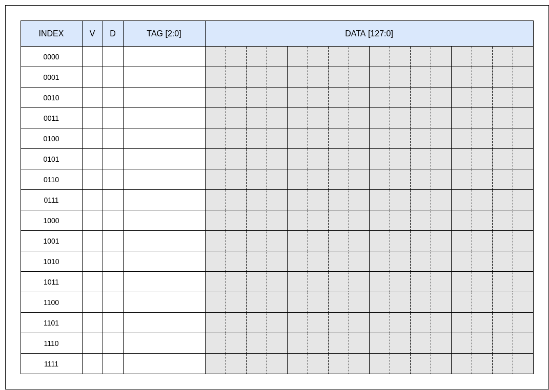
Data cache is implemented as a direct mapped cache and a cache block contains 16 bytes of data (4 words) and has 16 cache blocks. The implemented data cache can hold 256 bytes of data.
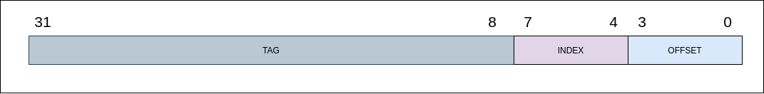
The input ADDRESS is separated into TAG, INDEX and OFFSET as the following figure.
In the case of a cache miss, until the data fetching from the data memory is completed,the cache controller will have to keep the signals sent to the memory in a stable state. A finite sate machine was used to implement the cache controller and the state diagram is shown in the following figure.